Data read-write method and control device of semiconductor processing equipment

A technology of data reading and writing and processing equipment, applied in the input/output process of data processing, electrical digital data processing, input/output to record carrier, etc., can solve the problem of occupying network communication resources, increasing system resource pressure, and reducing reading and writing Execution efficiency and other issues to achieve the effect of reducing CPU and memory consumption, avoiding reading and writing, and reducing communication pressure

Active Publication Date: 2021-04-06
BEIJING NAURA MICROELECTRONICS EQUIP CO LTD
View PDF7 Cites 2 Cited by
  • Summary
  • Abstract
  • Description
  • Claims
  • Application Information

AI Technical Summary

Problems solved by technology

[0003] Since semiconductor processing equipment usually includes a variety of control components such as flow control valves, mass flow controllers (MFC), vacuum pumps, heaters, etc., the amount of control signals is relatively large. However, the existing computer reads data every time It is necessary to read the data in the PLC memory as a whole, resulting in the data read this time including some redundant data that is not included in this requirement, which will not only occupy network communication resources and cause unnecessary communication pressure, but also cause the PC to Redundant data will be parsed, resulting in unnecessary CPU and memory consumption, increasing system resource pressure
In addition, when the PC writes data to the PLC memory, even a small amount of data needs to be written once alone, resulting in unnecessary communication pressure and reducing the efficiency of read and write execution

Method used


Image

  • Data read-write method and control device of semiconductor processing equipment
  • Data read-write method and control device of semiconductor processing equipment
  • Data read-write method and control device of semiconductor processing equipment

Examples


no. 1 example

[0046] see figure 1 The method for reading and writing data provided by the first embodiment of the present invention is applied to semiconductor processing equipment, for example, for performing read and write operations to a processor, such as a PLC for obtaining the status of control components of the semiconductor processing equipment.

[0047] Specifically, the above data reading and writing method includes the following steps:

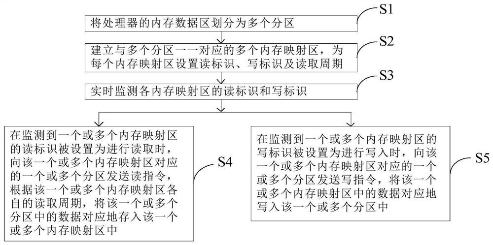
[0048] S1. Divide the memory data area of ​​the processor into multiple partitions;

[0049] Various factors may be considered comprehensively to divide the memory data area of ​​the above-mentioned processor, so as to achieve the purpose of reducing redundant data. These factors include but are not limited to: business logic, real-time requirements, related instruction issuing process and process monitoring process of each parameter (temperature, pressure, flow rate, etc.) in the process formula, and so on. Preferably, the partitioning is perf...

no. 2 example

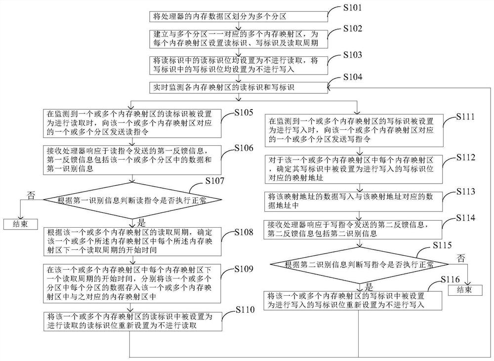
[0064] see figure 2 The data reading and writing method provided in this embodiment is a specific implementation manner of the above-mentioned first embodiment. Specifically, the data reading and writing method includes the following steps:

[0065] S101. Divide the memory data area of ​​the processor into multiple partitions;

[0066] S102. Establish a plurality of memory mapping areas corresponding to the plurality of partitions one-to-one, and set a read flag, a write flag, and a read cycle for each memory map area;

[0067] In this embodiment, a partition includes at least one data address, a memory mapping area corresponding to the partition includes at least one mapping address, and at least one data address corresponds to at least one mapping address. The read identification includes at least one read identification bit, the at least one read identification bit corresponds to the at least one mapping address, and the write identification includes at least one write id...

no. 3 example

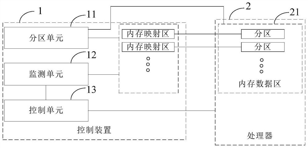
[0098] see image 3 , the embodiment of the present invention also provides a control device 1 for semiconductor processing equipment, the control device 1 includes:

[0099] The partition unit 11 is used to divide the memory data area 21 of the processor 2 into a plurality of partitions, and establish a plurality of memory mapping regions corresponding to the plurality of partitions one by one, and set a read flag, a write flag and a flag for each memory map region. read cycle;

[0100] The monitoring unit 12 is used for real-time monitoring of the read mark and write mark of each memory map area; and

[0101] The control unit 13 is configured to send a read instruction to one or more partitions corresponding to the one or more memory mapping areas when the monitoring unit 12 monitors that the read flag of one or more memory mapping areas is set to be read, According to the respective read cycles of the one or more memory-mapped areas, the data in the one or more partitions...


PUM


Abstract

The invention provides a data read-write method and a control device of semiconductor processing equipment. The data read-write method comprises the following steps: S1, dividing a memory data area of a processor into a plurality of partitions; s2, establishing a plurality of memory mapping regions in one-to-one correspondence with the plurality of partitions; s3, monitoring a read identifier and a write identifier of each memory mapping area in real time; s4, correspondingly storing the data in the one or more partitions into the one or more memory mapping regions according to respective reading periods of the one or more memory mapping regions when monitoring that the reading identifiers of the one or more memory mapping regions are set to be read; and S5, correspondingly writing the data in the one or more memory mapping regions into the one or more partitions when monitoring that the writing identifiers of the one or more memory mapping regions are set to be written. According to the data read-write method provided by the invention, the read-write of redundant data can be effectively avoided, so that the read-write execution efficiency can be improved.

Description

technical field [0001] The invention relates to the field of semiconductor manufacturing, in particular to a data reading and writing method and a control device for semiconductor processing equipment. Background technique [0002] Semiconductor processing equipment generally uses a combination of lower-level computers (such as PCs) and processors such as PLCs to control various hardware in the equipment. PCs and PLCs can use standards such as Ethernet (Ethernet) or field bus (DeviceNet) and other networks to achieve data communication, and the communication is mainly realized by reading and writing to the memory of the PLC. [0003] Since semiconductor processing equipment usually includes a variety of control components such as flow control valves, mass flow controllers (MFC), vacuum pumps, heaters, etc., the amount of control signals is relatively large. However, the existing computer reads data every time It is necessary to read the data in the PLC memory as a whole, re...

Claims


Application Information

Patent Timeline
Patent Type & Authority Applications(China)
IPC IPC(8): G06F3/06
CPCG06F3/061G06F3/0644G06F3/0655G06F3/0679
Inventor 高建强陆涛
Owner BEIJING NAURA MICROELECTRONICS EQUIP CO LTD
Why Eureka
Try Eureka