A Charge Pump with Wide Locking Range and Low Current Mismatch

A locking range and charge pump technology, applied in the field of microelectronics, can solve problems such as current mismatch, charge sharing, and restrictions on the application of charge pumps

Active Publication Date: 2022-07-01
CHONGQING UNIV OF POSTS & TELECOMM
View PDF19 Cites 0 Cited by
  • Summary
  • Abstract
  • Description
  • Claims
  • Application Information

AI Technical Summary

Problems solved by technology

figure 1 The traditional charge pump shown has problems such as charge sharing and current mismatch, which restrict the application of charge pumps in high-performance systems

Method used


Image

  • A Charge Pump with Wide Locking Range and Low Current Mismatch
  • A Charge Pump with Wide Locking Range and Low Current Mismatch
  • A Charge Pump with Wide Locking Range and Low Current Mismatch

Examples


Embodiment

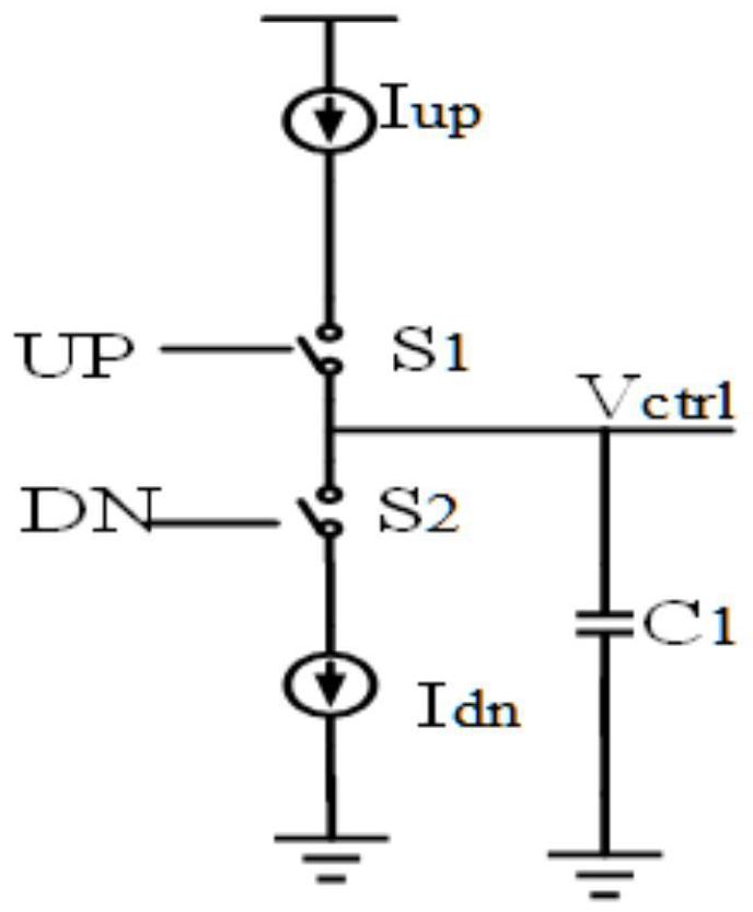
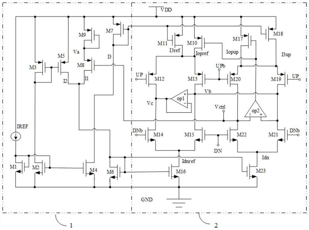
[0021] A wide locking range low current mismatch charge pump such as figure 2 As shown, it includes a charge pump bias circuit 1 and a charge pump core circuit 2;

[0022] The signal output terminal of the charge pump bias circuit 1 is connected to the signal input terminal of the charge pump core circuit 2 , and the signal output terminal of the charge pump core circuit 2 is connected to the signal input terminal of the charge pump bias circuit 1 . terminal; the charge pump bias circuit 1 provides a bias signal for the charge pump core circuit 2, and the charge pump core circuit 2 provides charge / discharge current for the filter capacitor of the subsequent circuit.

[0023] As a preferred technical solution, such as figure 2 As shown, the charge pump bias circuit 1 includes: reference current source IREF, NMOS transistor M1, NMOS transistor M2, PMOS transistor M3, NMOS transistor M4, PMOS transistor M5, NMOS transistor M6, PMOS transistor M7, PMOS transistor M8 and PMOS t...


PUM


Abstract

The present invention claims to protect a charge pump with a wide locking range and low current mismatch, including a charge pump bias circuit, a charge pump core circuit, and the like. The PMOS tube M9 of the charge pump bias circuit of the present invention is connected by a diode, and the gate of the PMOS tube M8 is connected to the output end of the charge pump. In the discharge state, the problem that the discharge current is small when the output voltage of the charge pump is low is compensated, and the output end of the charge pump is increased. Voltage dynamic range; in the core circuit of the charge pump, the error amplifier op1 is connected with unity gain, which can suppress the charge sharing effect at the moment of charge / discharge conversion; The gradual increase of the output voltage makes the gate voltage of the PMOS transistor M17 and the PMOS transistor M10 decrease, and the charging current increases, thereby increasing the dynamic range of the output voltage of the charge pump, thereby realizing a charge pump with a wide locking range and low current mismatch.

Description

technical field [0001] The invention belongs to the technical field of microelectronics, and in particular relates to a charge pump with wide locking range and low current mismatch. Background technique [0002] The charge pump is an important functional module of the delay-locked loop, and its performance directly affects the overall performance of the delay-locked loop. figure 1 It is a basic charge pump structure. When the switch S1 is closed and S2 is opened, the charging current source I UP When the capacitor C1 is charged, the voltage at the output terminal VCtrl of the charge pump rises; when the switch S1 is turned off and the switch S2 is turned on, the discharge current source I DN When the capacitor C1 is discharged, the voltage of the output terminal VCtrl of the charge pump drops; when the switch S1 and the switch S2 are turned on or off at the same time, the voltage of the output terminal VCtrl of the charge pump remains unchanged. figure 1 The conventional c...

Claims


Application Information

Patent Timeline
Patent Type & Authority Patents(China)
IPC IPC(8): H02M3/07
CPCH02M3/07
Inventor 周前能石头李红娟
Owner CHONGQING UNIV OF POSTS & TELECOMM
Why Eureka
Try Eureka