Multi-junction solar cell and manufacturing method thereof

A technology of solar cells and batteries, which is applied in circuits, photovoltaic power generation, electrical components, etc., and can solve the problems of low photoelectric conversion efficiency of components and large differences in current density, etc.

Active Publication Date: 2014-10-08
TIANJIN SANAN OPTOELECTRONICS
View PDF6 Cites 12 Cited by
  • Summary
  • Abstract
  • Description
  • Claims
  • Application Information

AI Technical Summary

Problems solved by technology

Although the bandwidth of energy absorption can be increased in this way, due to the stacking of semiconductor material layers with different energy gaps, the current density difference between the top solar cell

Method used


Image

  • Multi-junction solar cell and manufacturing method thereof
  • Multi-junction solar cell and manufacturing method thereof
  • Multi-junction solar cell and manufacturing method thereof

Examples


Embodiment Construction

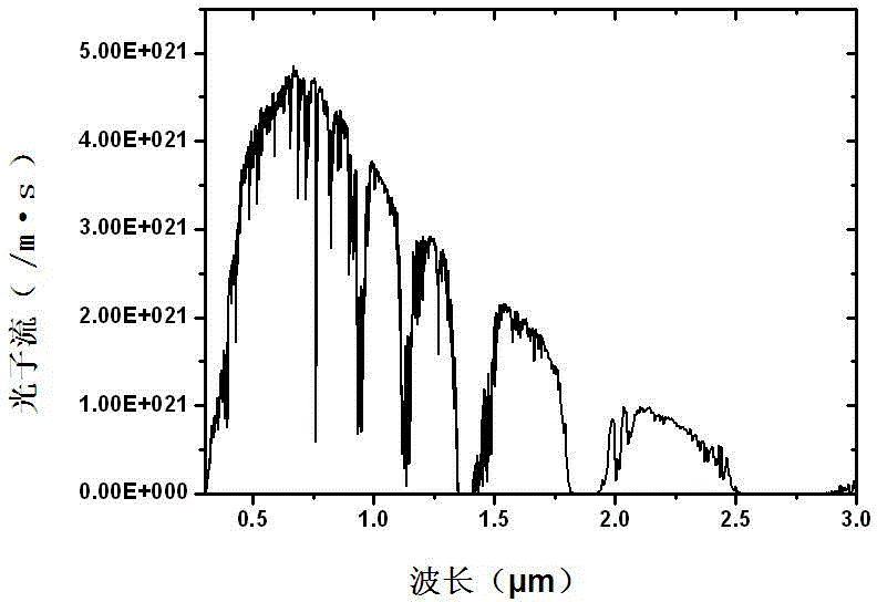
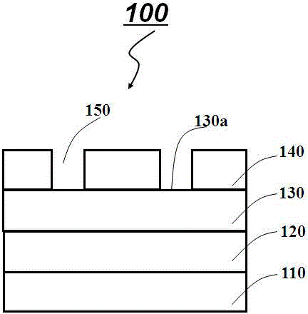
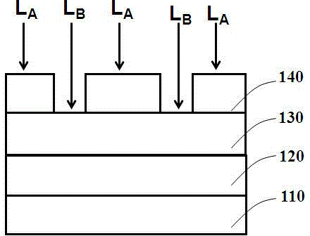
[0020] The multi-junction solar cell of the present invention reduces the light-receiving area of ​​the top sub-cell, reduces the current of the top sub-cell, and leaves the remaining light for the sub-cell below to absorb, increases the current of the bottom sub-cell, and finally reaches the multi-junction cell. Current matching, which is applicable to any multi-junction cells, such as GaInP / GaAs double-junction cells, GaInP / GaAs / Ge lattice matching triple-junction cells, GaInP / InGaAs / InGaAs triple-junction cells, AlGaInP / InGaAsP / InGaAs / Ge quadruple-junction cells Cells, GaInP / InGaAs / InGaAs / InGaAs four-junction cells, GaInP / InGaAs / InGaNAsSb / Ge four-junction cells, AlGaInP / AlGaAs / GaAs / InGaNAs / Ge five-junction cells, etc. In general, the current limiting value of the sub-cell under the multi-junction solar cell is 5%~20%, so the light-receiving area of ​​the top cell can be limited to 70%~97% of the total area. The implementation of the presen...


PUM


Abstract

The invention provides a multi-junction solar cell. The multi-junction solar cell at least comprises a bottom sub-cell and a top sub-cell, wherein the top sub-cell is located on the bottom sub-cell. The top sub-cell is only formed on a part of the surface of the bottom sub-cell so that the light receiving area of the top sub-cell can be reduced. When light enters the multi-junction solar cell, a part of the light is directly absorbed by other sub-cells below the top sub-cell, so that a current of the top sub-cell is reduced.

Description

technical field [0001] The invention belongs to the field of compound semiconductor solar cells, and in particular relates to a multi-junction solar cell structure and a preparation method thereof. Background technique [0002] A solar cell is a semiconductor device that uses the photovoltaic effect to convert solar energy into electrical energy. It is composed of a p-type and n-type semiconductor. When sunlight irradiates the device, the sunlight with energy greater than the energy gap of the semiconductor will be absorbed, causing the semiconductor device to generate electron-hole pairs, which will form a current when it is turned on. [0003] figure 1 It is a spectrum map of solar radiation, the main wavelength distribution ranges from 0.3 microns of ultraviolet light to several microns of infrared light, converted into photon energy, from about 0.4 eV to 4 eV. In order to be able to absorb more sunlight energy, multi-junction solar cells have been proposed, which stack...

Claims


Application Information

Patent Timeline
IPC IPC(8): H01L31/0725H01L31/0352H01L31/18
CPCY02E10/50H01L31/0304H01L31/0725H01L31/0735H01L31/1828H01L31/0352H01L31/18Y02E10/543Y02E10/544Y02P70/50
Inventor 宋明辉林桂江陈文浚毕京锋
Owner TIANJIN SANAN OPTOELECTRONICS
Why Eureka
Try Eureka