Multi-junction solar cells and methods of making the same

A technology of solar cells and batteries, applied in circuits, photovoltaic power generation, electrical components, etc., can solve problems such as excessive differences in current density and low photoelectric conversion efficiency of components

Active Publication Date: 2017-01-18
TIANJIN SANAN OPTOELECTRONICS
View PDF5 Cites 0 Cited by
  • Summary
  • Abstract
  • Description
  • Claims
  • Application Information

AI Technical Summary

Problems solved by technology

Although the bandwidth of energy absorption can be increased in this way, due to the stacking of semiconductor material layers with different energy gaps, the current density difference between the top solar cell and the bottom solar cell is too large, and this current mismatch will cause the entire The photoelectric conversion efficiency of the device is reduced, so how to reduce the current mismatch is an important issue

Method used


Image

  • Multi-junction solar cells and methods of making the same
  • Multi-junction solar cells and methods of making the same
  • Multi-junction solar cells and methods of making the same

Examples


no. 1 example GaI

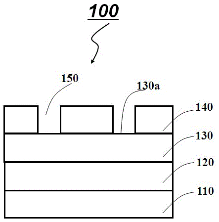
[0021] figure 2 A side cross-sectional view of a GaInP / GaAs / Ge triple-junction solar cell 100 according to a first embodiment of the present invention is shown.

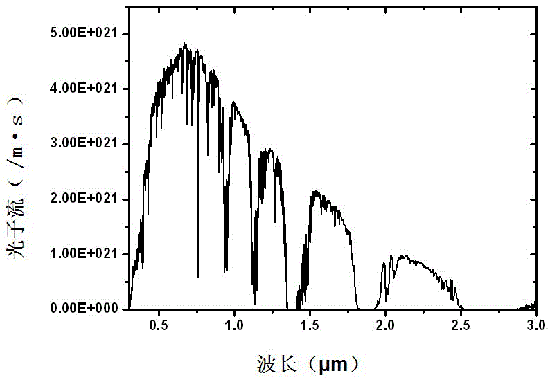
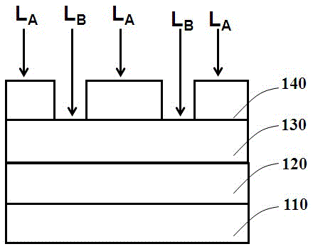
[0022] Please see figure 2 , a triple-junction solar cell 100 , including a p-type Ge substrate 110 , a first Ge sub-cell 120 , a second GaAs sub-cell 130 , and a third GaInP sub-cell 140 . Generally, the first and second sub-cells, and the second and third sub-cells are respectively connected through tunnel junctions (not shown in the figure). Wherein the third GaInP sub-cell 140 has a groove pattern 150, which exposes part of the surface 130a of the second GaAs sub-cell 130 below it. Please see attached image 3 , when the solar cell is placed in the sunlight environment, the light L A Incident to the surface of the third sub-cell 140, absorbed by the third sub-cell, light L B When it is incident on the groove pattern, it is directly absorbed by the GaAs second sub-cell 130 below the groove.

[0023] Please...


PUM


Abstract

A multi-junction solar cell, at least comprising a bottom sub-cell and a top sub-cell located on the bottom sub-cell. The top sub-cell is merely formed on a partial surface of the bottom sub-cell to reduce a light receiving area of the top sub-cell; and when light is incident onto the multi-junction solar cell, partial light is directly absorbed by the rest of the sub-cells under the top sub-cell, so as to reduce a current of the top sub-cell.

Description

technical field [0001] The invention belongs to the field of compound semiconductor solar cells, and in particular relates to a multi-junction solar cell structure and a preparation method thereof. Background technique [0002] A solar cell is a semiconductor device that uses the photovoltaic effect to convert solar energy into electrical energy. It is composed of a p-type and n-type semiconductor. When sunlight irradiates the device, the sunlight with energy greater than the energy gap of the semiconductor will be absorbed, causing the semiconductor device to generate electron-hole pairs, which will form a current when it is turned on. [0003] figure 1 It is a spectrum map of solar radiation, the main wavelength distribution ranges from 0.3 microns of ultraviolet light to several microns of infrared light, converted into photon energy, from about 0.4 eV to 4 eV. In order to be able to absorb more sunlight energy, multi-junction solar cells have been proposed, which stack...

Claims


Application Information

Patent Timeline
Patent Type & Authority Patents(China)
IPC IPC(8): H01L31/0725H01L31/0352H01L31/18
CPCH01L31/0304H01L31/0725H01L31/0735H01L31/1828H01L31/0352H01L31/18Y02E10/543Y02E10/544Y02P70/50
Inventor 宋明辉林桂江陈文浚毕京锋
Owner TIANJIN SANAN OPTOELECTRONICS
Why Eureka
Try Eureka