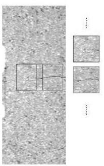
Surface defect detection method and device and computer readable storage medium
A defect detection and defect technology, which is applied in the field of image recognition, can solve the problems that the detection method cannot meet the requirements and the surface defect image data is small, and achieve the effect of solving the problem of small area defect detection, increasing the amount of training data, and avoiding proportional imbalance
- Summary
- Abstract
- Description
- Claims
- Application Information
AI Technical Summary
Problems solved by technology
Method used
Image
Examples
Embodiment 1
[0049] For a surface defect method provided by the first embodiment of the present invention, please refer to figure 1 , the method includes step S01 to step S07:
[0050] Step S001, collecting surface images of industrial parts.
[0051]Use professional acquisition equipment to collect images on the surface of industrial parts. The surface of each part should be captured as several non-overlapping images. In order to ensure the high quality of the image, the parts should be photographed in a controlled environment, and the high resolution should be ensured to avoid the loss of tiny cracks or other defects due to pixel problems. For example, an industrial image acquisition system composed of a host computer, an industrial camera, an LED light source, and a photoelectric sensor. Its working process is: first initialize the equipment and self-check the equipment, and then the host computer drives the industrial camera (area array CCD sensor) through software, but the industria...
Embodiment 2
[0063] In another embodiment of the present invention, the images collected by collecting the surface images of industrial parts include images with defects and images without defects.
[0064] By collecting both defective and non-defective images, training on both defective and non-defective images can increase the amount of data and improve the judgment accuracy of the defect detection network.
Embodiment 3
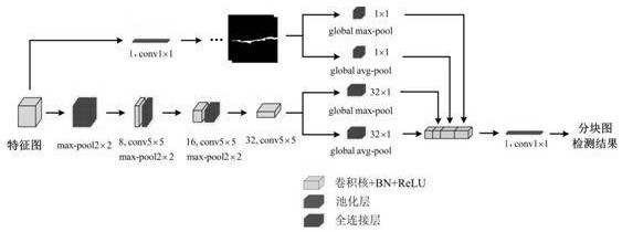
[0066] In one embodiment of the invention, see image 3 , the construction of the defect detection network includes steps S031-S032:
[0067] Step S031, building a segmentation network, the segmentation network is composed of a convolutional layer, a pooling layer and a fully connected layer.
[0068] Such as Figure 4 Schematic diagram of the segmentation network shown, which consists of convolutional layers, pooling layers, and fully connected layers. The size of the convolution kernel and the number of convolution layers can be changed according to the size of the image block, but in order to capture the small feature details in the image, this segmentation network needs to use a large convolution kernel in a relatively deep layer, and all convolutions The step size of the product kernel is set to 1. The segmentation network of the present invention uses the pooling layer to complete the downsampling operation, and uses the pooling layer to replace the convolutional laye...
PUM
 Abstract
Description
Claims
Application Information
 - R&D
- Intellectual Property
- Life Sciences
- Materials
- Tech Scout
- Unparalleled Data Quality
- Higher Quality Content
- 60% Fewer Hallucinations
Browse by: Latest US Patents, China's latest patents, Technical Efficacy Thesaurus, Application Domain, Technology Topic, Popular Technical Reports.
© 2025 PatSnap. All rights reserved.Legal|Privacy policy|Modern Slavery Act Transparency Statement|Sitemap|About US| Contact US: help@patsnap.com


