Check patentability & draft patents in minutes with Patsnap Eureka AI!

A terahertz detector integrated with silicon photonic crystal microcavity

A terahertz detector and photonic crystal microcavity technology, applied in the field of terahertz detection, can solve the problems of deteriorating antenna performance, difficulty in resonant frequency control, unsatisfactory resonant frequency selection effect, etc., achieve small loss, improve sensitivity, and Q value high effect

Active Publication Date: 2022-05-17
NANJING UNIV
View PDF4 Cites 0 Cited by
  • Summary
  • Abstract
  • Description
  • Claims
  • Application Information

AI Technical Summary

Problems solved by technology

However, there are many limitations in the antenna coupling structure. For example, the substrate interference effect will deteriorate the performance of the antenna. The integration of the antenna often needs to consider the impedance matching with the detector. More importantly, the detector of the antenna coupling structure is limited by the substrate FP cavity, and the resonance The frequency selection effect is not ideal, and the resonance frequency control is very difficult

Method used


Image

  • A terahertz detector integrated with silicon photonic crystal microcavity
  • A terahertz detector integrated with silicon photonic crystal microcavity
  • A terahertz detector integrated with silicon photonic crystal microcavity

Examples


Embodiment approach

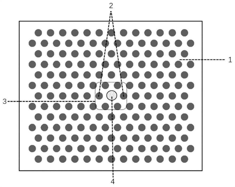
[0025] As a preferred embodiment, the two-dimensional photonic crystal plate 1 is formed by drilling circular air holes on a high-resistance silicon wafer, and the radii of the circular air holes on each crystal unit are the same.

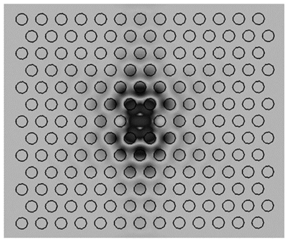
[0026] As a preferred embodiment, the L1-type photonic microcavity 3 removes one lattice from the photonic crystal plate to form a microcavity, and the microcavity is surrounded by at least six layers of lattices. Further preferably, the L1-type photonic microcavity 3 adjusts the offset of the lattice at both ends of the microcavity to realize the detection of dual-band terahertz waves, wherein the offset is 0.1-0.3a, where a is the triangular lattice constant. The L1 photonic microcavity 3 is located at the center of the two-dimensional photonic crystal plate 1 .

[0027] As a preferred embodiment, the terahertz detector is a microbolometer, a field effect tube, a pyroelectric diode or a Schottky diode. Further preferably, the terahertz detector ...

Embodiment

[0034] In order to verify the effectiveness of the solution of the present invention, the following simulation experiments are carried out.

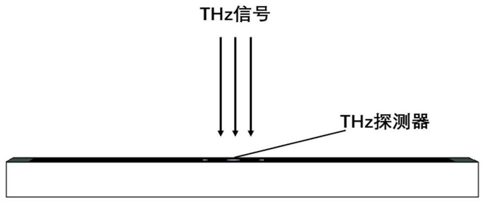
[0035] Such as figure 1 As shown, this embodiment provides a terahertz detector integrated with a silicon photonic crystal microcavity, including:

[0036] The two-dimensional photonic crystal plate 1 is formed by punching circular air holes on a high-resistance silicon wafer, arranged periodically to form a triangular lattice structure, and the radius of the circular air holes is the same.

[0037] An L1-type photonic microcavity 3 located on a photonic crystal plate, wherein the L1-type photonic microcavity 3 removes an air hole on the photonic crystal plate to form a microcavity, and the microcavity is surrounded by at least six layers of lattice. Offset air through holes 2 on both sides of the microcavity, and a terahertz detector 4 in the center of the microcavity. The thickness of the two-dimensional photonic crystal plate is set...


PUM

PropertyMeasurementUnit
refractive indexaaaaaaaaaa

Abstract

The present invention proposes a terahertz detector integrating a silicon photonic crystal microcavity, including a two-dimensional photonic crystal plate, an L1 photonic microcavity and a terahertz detector, wherein: the lattices on the two-dimensional photonic crystal plate are arranged periodically to form a triangle Lattice structure, L1-type photonic microcavity is set on the two-dimensional photonic crystal plate, and terahertz detectors are prepared by micro-nano processing on the L1-type photonic microcavity. Compared with the antenna coupling structure, the photonic crystal microcavity coupling structure of the present invention has smaller loss, higher efficiency, higher resonance quality factor, eliminates the interference of the substrate effect of the terahertz detector, and improves the sensitivity of the detector.

Description

technical field [0001] The invention relates to a terahertz detection technology, in particular to a terahertz detector integrated with a silicon photonic crystal microcavity. Background technique [0002] The terahertz spectrum usually refers to the spectrum region between 0.1THz and 10THz, corresponding to a wavelength of 30-3000μm. Its special spectral position determines its superiority in biological imaging and high-speed wireless communication compared to other bands. The current progress of terahertz technology urgently requires high-power sources and high-sensitivity detectors. To improve the sensitivity of the detector, in addition to directly improving the intrinsic performance of the detector, we can also start with the coupling strength between the terahertz detector and the signal. The traditional solution uses an integrated planar antenna coupling structure, which receives a fixed frequency signal through the antenna, transmits it to the antenna feeding point,...

Claims


Application Information

Patent Timeline
Patent Type & Authority Patents(China)
IPC IPC(8): G01J1/42G02B6/122G02B6/293
CPCG01J1/42G02B6/29335G02B6/1225Y02P70/50
Inventor 涂学凑张祎琛周淑宇蒋成涛贾小氢赵清源张蜡宝康琳陈健吴培亨
Owner NANJING UNIV
Features
  • R&D
  • Intellectual Property
  • Life Sciences
  • Materials
  • Tech Scout
  • Unparalleled Data Quality
  • Higher Quality Content
  • 60% Fewer Hallucinations
Learn More