
Light collecting device and optical lens

A light collection and optical lens technology, applied in optics, instruments, televisions, etc., can solve the problem of low light collection efficiency

Active Publication Date: 2021-05-07
ZHEJIANG LAB
View PDF15 Cites 0 Cited by
  • Summary
  • Abstract
  • Description
  • Claims
  • Application Information

AI Technical Summary

Problems solved by technology

[0006] In view of this, the object of the present invention is to propose a light collection device and an optical lens, which can overcome the defect of low light collection efficiency caused by the packaging space inside the lens being filled with a low refractive index medium in the prior art, and improve the performance of the lens. Overall quality

Method used


Image

  • Light collecting device and optical lens
  • Light collecting device and optical lens

Examples


Embodiment Construction

[0023] The present invention will be described in detail below in conjunction with the specific embodiments shown in the accompanying drawings, but these embodiments do not limit the present invention, those of ordinary skill in the art make structural, method, or functional changes based on these embodiments All are included in the scope of protection of the present invention.

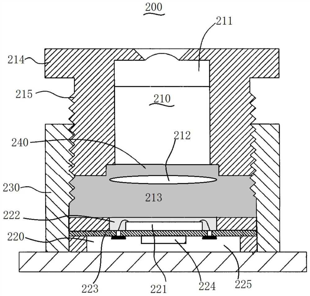
[0024] See figure 2 , figure 2 It is a light collection device 200 of the present invention, including a lens module 210 , a photoreceptor module 220 and a base frame 230 . The base frame 230 provides an accommodating space and a housing for the lens module 210 and the photoreceptor module 220 to be installed. The device module 220 is disposed on the lower portion of the base frame 230 .

[0025] Specifically, the lens module 210 includes an optical lens group 211 and an objective lens 212 . The optical lens group 211 is shown in a simplified manner in the figure. In practice, the optical lens g...


PUM


Abstract

The invention provides a light collecting device and an optical lens, the light collecting device comprises an optical lens group, an objective lens, a photosensitive chip and a chip packaging layer, part or all of the optical lens group and the objective lens are arranged in a first sealing cavity, the photosensitive chip and the chip packaging layer are arranged in a second sealing cavity, and the chip packaging layer is arranged in the second sealing cavity. The first sealing cavity and the second sealing cavity are connected into a whole, optical matching liquid is arranged in the first sealing cavity, the objective lens is immersed in the optical matching liquid, the optical matching liquid is in contact with the chip packaging layer, and the refractive index of the optical matching liquid is larger than that of air and close to that of the chip packaging layer. According to the invention, the optical matching liquid close to the packaging layer is arranged in the optical lens of the lens, so that the collection efficiency of light in the lens is improved.

Description

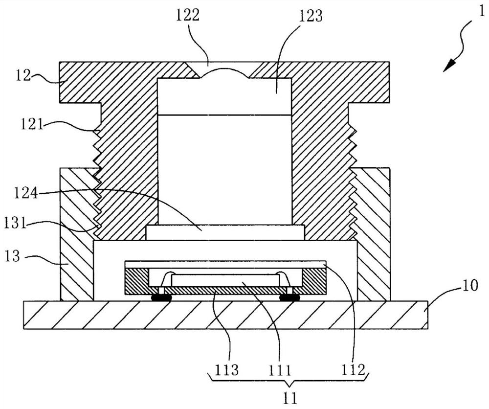
technical field [0001] The invention relates to the technical field of optical imaging, in particular to an optical lens and a light collection device. Background technique [0002] The light collection efficiency plays an important role in the optical system, which determines the imaging quality or detection efficiency of the system. However, the traditional detection window chip is located in a low-refractive-index space (air or other gases), and the detection efficiency is low. [0003] see figure 1 As shown in FIG. 2 , it is a schematic cross-sectional view of a package structure of a conventional micro lens module (Compact Camera Module, CCM for short). The existing micro lens module packaging structure 1 includes: a substrate 10 , a sensing chip module 11 , a lens barrel 12 , and a bearing seat 13 . The sensing chip module 11 further includes: an image sensing chip 111 , a transparent cover 112 and a chip carrier 113 . [0004] The sensing chip module 11 is bonded ...

Claims


Application Information

Patent Timeline
IPC IPC(8): H04N5/225G03B17/04
CPCG03B17/04H04N23/55
Inventor 石岩陈建勇金尚忠陈义赵天琦徐睿
Owner ZHEJIANG LAB
Learn More