Software-defined on-chip system, data interaction method and system architecture

A software-defined, system-data technology, applied in the fields of electrical digital data processing, special data processing applications, electrical components, etc., can solve the problem of difficult to meet the needs of complex and diverse application tasks, limited flexibility and scalability, and very different computing performance. major problems, to achieve the effect of fast reconstruction, great flexibility, and improved reliability

Active Publication Date: 2021-05-14
CHINA NAT DIGITAL SWITCHING SYST ENG & TECHCAL R&D CENT +1
View PDF7 Cites 6 Cited by
  • Summary
  • Abstract
  • Description
  • Claims
  • Application Information

AI Technical Summary

Problems solved by technology

[0003] Since different types of application tasks have different computing characteristics, the requirements for computing-storage-communication resources are also different, and multiple types of parallelism, different limitations, and different communication and synchronization requirements may be mixed within application tasks. The computing performance of the same application on different architectures will vary greatly. Therefore, it is necessary for the application to adapt to the solidified system structure from the perspective of function and performance. The flexibility and scalability are poor and have great limitations. Application performance It will also be greatly reduced, and it is difficult to meet the complex and diverse application task requirements

Method used


Image

  • Software-defined on-chip system, data interaction method and system architecture
  • Software-defined on-chip system, data interaction method and system architecture
  • Software-defined on-chip system, data interaction method and system architecture

Examples


Embodiment Construction

[0023] In order to make the purpose, technical solution and advantages of the present invention more clear and understandable, the present invention will be further described in detail below in conjunction with the accompanying drawings and technical solutions.

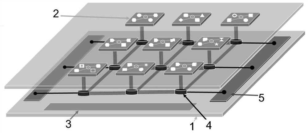
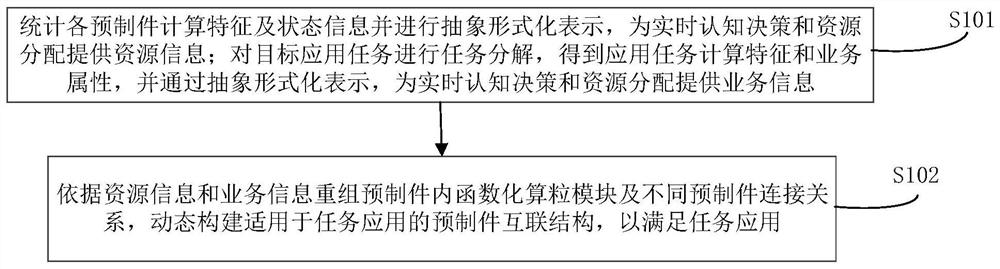
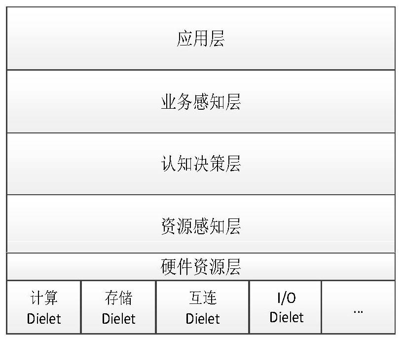
[0024] Embodiment of the present invention, see figure 1 As shown, a software-defined on-chip system is provided, including: a wafer-level interconnection substrate, several prefabricated parts arranged on the wafer-level interconnection substrate, and a software-defined on-die chip for interconnection between different prefabricated parts Interconnection network, each prefabricated part is integrated with different functional computing particles according to the functional requirements of the field application; the prefabricated parts follow the unified interface standard and physical layer protocol specification, and are connected to each other through the wafer-level interconnection substrate and software-defined on...


PUM


Abstract

The invention belongs to the technical field of semiconductors, and particularly relates to a software-defined on-chip system, a data interaction method and a system architecture, the system comprises a wafer-level interconnection substrate, a plurality of prefabricated members arranged on the wafer-level interconnection substrate, and a software-defined on-chip interconnection network used for interconnection among different prefabricated members, each prefabricated member is integrated with different function calculation particles according to field application function requirements; the prefabricated members follow a unified interface standard and a physical layer protocol specification, and data exchange is carried out between the prefabricated members through a wafer-level interconnection substrate and a software-defined on-chip interconnection network, so that different function calculation particles are recombined and/or rebuilt in a software-defined mode to adapt to different application requirements and task mapping requirements. According to the method, boundary conditions such as a design method, a calculation normal form, an implementation material and an integration mode of an existing integrated circuit are broken through, and flexible interconnection and functional reconstruction of different prefabricated members for field application are realized, so that complex and diversified application task requirements are met.

Description

technical field [0001] The invention belongs to the technical field of semiconductors, and in particular relates to a software-defined on-chip system, a data interaction method, and a system architecture. Background technique [0002] With the gradual failure of Moore's Law and Dennard's scaling law, the traditional engineering technology route based on the layer-by-layer stacking system of devices, components, modules, and racks has encountered a sustainable development bottleneck. At present, the chip process is getting closer and closer to the quantum effect area, the number of transistors per unit area is increasing, the yield control is becoming more and more difficult, the problem of power consumption is becoming more and more prominent, and the manufacturing and design costs are rising exponentially. Single-chip performance improvement has approached the ceiling. At the same time, when continuing to use the traditional engineering technology route of "stacking" devic...

Claims


Application Information

Patent Timeline
Patent Type & Authority Applications(China)
IPC IPC(8): G06F30/398H01L27/02
CPCG06F30/398H01L27/0207
Inventor 邬江兴刘勤让汤先拓沈剑良吕平刘冬培董春雷陈艇宋克高彦钊
Owner CHINA NAT DIGITAL SWITCHING SYST ENG & TECHCAL R&D CENT
Why Eureka
Try Eureka