LED dimming control circuit, chip, lighting device and dimming control method
A dimming control circuit, LED light string technology, applied in the direction of energy-saving control technology, electrical components, etc., can solve the problems of flicker, poor dimming accuracy, single dimming effect, etc., achieve ultra-low standby power consumption, eliminate flicker effect of the phenomenon
- Summary
- Abstract
- Description
- Claims
- Application Information
AI Technical Summary
Problems solved by technology
Method used
Image
Examples
Embodiment 1
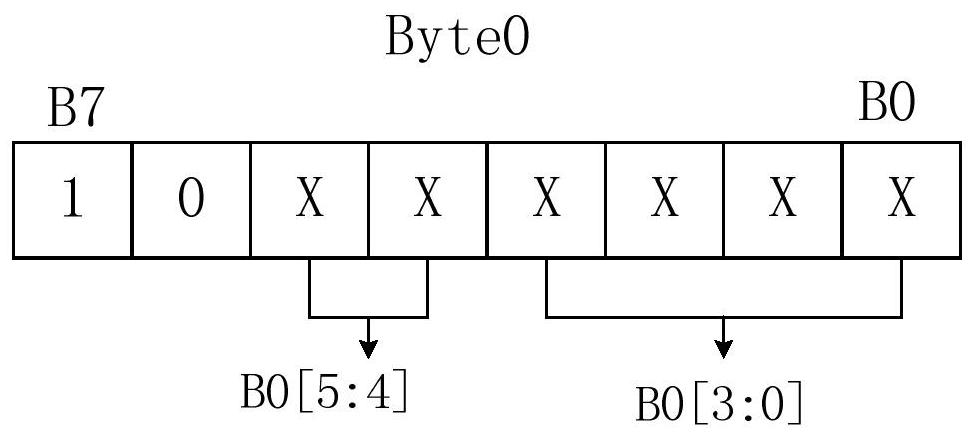
[0059] Embodiment 1: realize that the LED dimming control chip 71 enters the sleep mode (Sleep Mode), and does not perform dimming operation. Specifically, the input procedure of the MCU is as follows:
[0060] Start: 10000000 (write to Byte0, where B0[5:4]=00 to enter Sleep mode)
[0061] Stop.
Embodiment 2
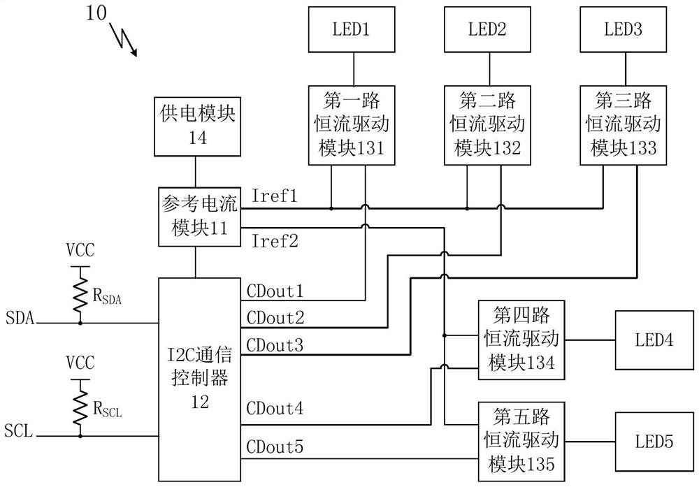
[0062] Embodiment 2: Realize the simultaneous output of 5 output channels OUT1~OUT5; the maximum current of OUT1~OUT3 is 40mA, the grayscale of OUT1 is 2 / 1024, the grayscale of OUT2 is 512 / 1024, and the grayscale of OUT3 is 1022 / 1024; the maximum current of OUT4~OUT5 is 60mA , OUT4 grayscale 512 / 1024, OUT5 grayscale 1022 / 1024. Specifically, the input procedure of the MCU is as follows:
[0063] Start: 10110000 (write to Byte0, OUT1~OUT5 output at the same time, select Byte1)
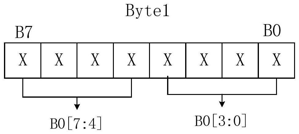
[0064] 01001100 (write to Byte1, set the range current of OUT1~OUT3 to 40mA, and the range current of OUT4~OUT5 to 60mA)
[0065] 10100010 (write to Byte2)
[0066] 10100000 (write to Byte3, Byte2 and Byte3 together set OUT1 grayscale 2 / 1024)
[0067] 10100000 (write to Byte4)
[0068] 10110000 (write Byte5, Byte4 and Byte5 together set OUT2 grayscale 512 / 1024)
[0069] 10111110 (write Byte6)
[0070] 10111111 (write to Byte7, Byte6 and Byte7 together set OUT3 grayscale 1022 / 1024)
[0071] 10100000 ...
Embodiment 3
[0076] Embodiment 3: Realize the simultaneous output of selected output channels OUT4~OUT5; the maximum current of OUT4~OUT5 is 60mA, the grayscale of OUT4 is 2 / 1024, the grayscale of OUT5 is 512 / 1024; after 1mS, the grayscale of OUT4 is 512 / 1024, and the grayscale of OUT5 is 2 / 1024. Specifically, the input procedure of the MCU is as follows:
[0077] Start1: 10100000 (write to Byte0, OUT4~OUT5 output at the same time, select Byte1)
[0078] 00001100 (write to Byte1, set the range current of OUT1~OUT3 to 0mA, and the range current of OUT4~OUT5 to 60mA)
[0079] Stop1 (here indicates the interval between frames)
[0080] Start2: 10100111 (write Byte0, OUT4~OUT5 output at the same time, select Byte8)
[0081] 10100010 (write Byte8)
[0082] 10100000 (write to Byte9, Byte8 and Byte9 together set OUT4 grayscale 2 / 1024)
[0083] 10100000 (write Byte10)
[0084] 10110000 (write Byte11, Byte10 and Byte11 together set OUT5 grayscale 512 / 1024)
[0085] Stop2
[0086] Start3: 1...
PUM
 Abstract
Description
Claims
Application Information
 - R&D
- Intellectual Property
- Life Sciences
- Materials
- Tech Scout
- Unparalleled Data Quality
- Higher Quality Content
- 60% Fewer Hallucinations
Browse by: Latest US Patents, China's latest patents, Technical Efficacy Thesaurus, Application Domain, Technology Topic, Popular Technical Reports.
© 2025 PatSnap. All rights reserved.Legal|Privacy policy|Modern Slavery Act Transparency Statement|Sitemap|About US| Contact US: help@patsnap.com


