Black matrix substrate and display device equipped with black matrix substrate

A technology of black matrix and black matrix layer, which is applied in the direction of identification devices, lighting devices, instruments, etc., can solve the problems of not considering the composition of color filters, etc., and achieve the effect of improving display contrast

Pending Publication Date: 2021-06-04
TOPPAN PRINTING CO LTD
View PDF16 Cites 2 Cited by
  • Summary
  • Abstract
  • Description
  • Claims
  • Application Information

AI Technical Summary

Problems solved by technology

Patent Document 2 does not consider a

Method used


Image

  • Black matrix substrate and display device equipped with black matrix substrate
  • Black matrix substrate and display device equipped with black matrix substrate
  • Black matrix substrate and display device equipped with black matrix substrate

Examples


no. 1 approach

[0060] (Black Matrix Substrate)

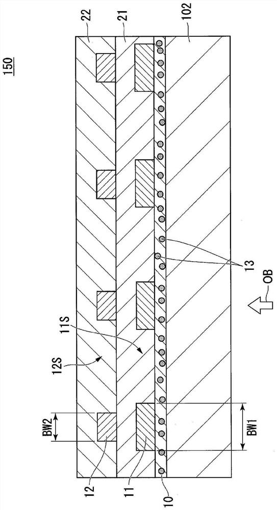
[0061] figure 1 It is a cross-sectional view partially showing the black matrix substrate of the first embodiment of the present invention.

[0062] The black matrix substrate 150 has: a transparent substrate 102; a semi-permeable film 10 formed on the transparent substrate 102; The first black matrix layer 11 on 10; the first transparent resin layer 21 (transparent resin layer) formed on the semi-permeable film 10 in a manner covering the first black matrix layer 11; formed on the first transparent resin layer 21 and the second transparent resin layer 22 formed on the first transparent resin layer 21 in such a way as to cover the second black matrix layer 12 .

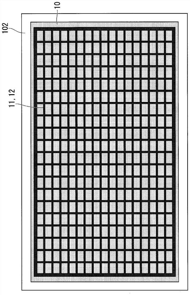
[0063] That is, the black matrix substrate 150 has a structure in which the semi-permeable film 10, the first black matrix layer 11, the first transparent resin layer 21, the second black matrix layer 12, and the second transparent resin layer 22 are sequentially stacked on the tran...

Deformed example 1

[0139] Figure 7 It is a cross-sectional view partially showing Modification 1 of the black matrix substrate according to the embodiment of the present invention. At the point that the semi-permeable film 10 uses a semi-permeable film to which no optically isotropic particles 13 are added, Figure 7 The black matrix substrate 550 shown with figure 1 The black matrix substrate 150 shown is different.

[0140] According to such a black matrix substrate 550, not only the same effect as that of the above-mentioned first embodiment can be obtained, but also because no particles 13 are added to the semi-permeable film 10, the structure of the semi-permeable film 10 becomes simple, which contributes to The cost of the black matrix substrate is reduced.

Deformed example 2

[0142] Figure 8 It is a cross-sectional view partially showing Modification 2 of the black matrix substrate according to the embodiment of the present invention. At the point of providing the colored layers of the red layer R, the green layer G, and the blue layer B, Figure 8 The black matrix substrate 650 shown with figure 1 The black matrix substrate 150 shown is different.

[0143] Each of the plurality of first pixel openings 11S of the first black matrix layer 11 has a colored layer CF. The colored layer CF is composed of a red layer R, a green layer G, and a blue layer B. The red layer R, the green layer G, and the blue layer B are disposed in the first pixel opening portion 11S in such a manner as to correspond to the three first pixel opening portions 11S.

[0144] In particular, the red layer R, the green layer G, and the blue layer B are provided in the first pixel opening 11S of the first black matrix layer 11 between the first transparent resin layer 21 and t...


PUM

PropertyMeasurementUnit
Particle sizeaaaaaaaaaa

Abstract

A black matrix substrate according to the present invention comprises: a transparent substrate; a semi-transmissive film formed on the transparent substrate; a first black matrix layer formed on the semi-transmissive film in contact with the semi-transmissive film in the thickness direction of the semi-transmissive film, the first black matrix layer having a plurality of first openings; a transparent resin layer formed on the semi-transmissive film to cover the first black matrix layer; and a second black matrix layer formed on the transparent resin layer and having a plurality of second openings. The semi-transmissive film overlaps the plurality of first openings and the first black matrix layer in a plan view viewed from the side opposite the side of the transparent substrate on which the semi-transmissive film is formed, and the positions of the plurality of second openings correspond to the positions of the plurality of first openings in the plan view.

Description

technical field [0001] The present invention relates to a black matrix substrate used in a liquid crystal display device, a micro LED (LED display), an organic EL display device, and the like, and a display device including the black matrix substrate. Background technique [0002] The liquid crystal display device is a display device using a backlight using LED (Light Emitting Diode, Light Emitting Diode) as a light source, and using liquid crystal as a display function layer for switching between transmission and non-transmission of light. [0003] In recent years, attention has been paid to techniques for applying direct-type backlights called mini LEDs, in which a plurality of LED chips of about 5 μm to 100 μm in size are arranged in a matrix, to liquid crystal display devices. In mini LEDs, three kinds of LED chips that emit red light, green light, and blue light are usually used. [0004] In addition, attention has been paid to techniques for partially adjusting the em...

Claims


Application Information

Patent Timeline
IPC IPC(8): G09F9/30G02B5/20G02F1/1335G02F1/1362H01L27/32H01L51/50H05B33/02
CPCG02B5/20G02F1/1335G02F1/1362G09F9/30H05B33/02H10K59/00H10K50/00G02B5/201G02B5/223G02B1/04G02B5/208G02B5/206H10K59/126H10K50/865
Inventor 山内淳福吉健蔵
Owner TOPPAN PRINTING CO LTD
Why Eureka
Try Eureka