Central processing unit and manufacturing method thereof

A central processing unit and buffer technology, applied in the semiconductor field, can solve problems such as poor CPU performance

Active Publication Date: 2021-06-08
YANGTZE ADVANCED MEMORY INDUSTRIAL INNOVATION CENTER CO LTD
View PDF4 Cites 5 Cited by
  • Summary
  • Abstract
  • Description
  • Claims
  • Application Information

AI Technical Summary

Problems solved by technology

However, limited by the capacity and volume of SRAM, the performance of CPU is not good
Simultaneous improvement of CPU performance and size integration has become a challenge

Method used


Image

  • Central processing unit and manufacturing method thereof
  • Central processing unit and manufacturing method thereof
  • Central processing unit and manufacturing method thereof

Examples


Embodiment Construction

[0079] In order to make the technical solutions and advantages of the embodiments of the present invention more clear, the specific technical solutions of the invention will be further described in detail below in conjunction with the drawings in the embodiments of the present invention.

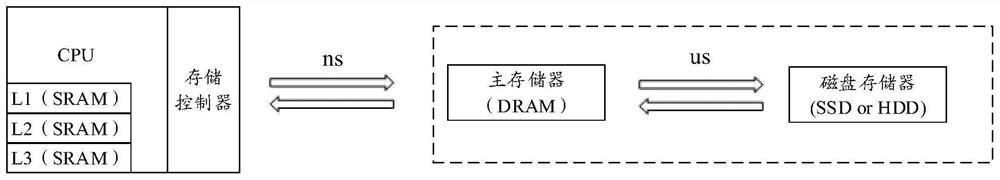
[0080] Due to the huge difference in storage speed and cost of different storage technologies, in order to access data efficiently, in the computer storage system, the most commonly used data is placed on the storage device with a fast reading and storage speed, and the infrequently used data is placed on the storage device with a fast reading and storage speed. on slow storage devices. A memory system is a hierarchy of storage devices with varying capacities, costs, and access times. Such as Figure 1a As shown, the buffer memory, main memory, and disk storage capacity of the CPU arranged from left to right are getting larger and larger, but the access speed is getting slower and slower. F...


PUM


Abstract

The embodiment of the invention provides a central processing unit (CPU) and a manufacturing method thereof. The CPU comprises a first semiconductor structure, and the first semiconductor structure comprises at least one core, first to (N-1) th levels of buffers in signal connection with the core, and a first bonding layer comprising a first conductive contact; wherein N is equal to three or four; The CPU also comprises a second semiconductor structure which comprises an Nth level buffer and a second bonding layer comprising a second conductive contact; the Nth level of buffer comprises a three-dimensional phase change memory; the three-dimensional phase change memory comprises a plurality of storage units; each storage unit comprises a first electrode layer, a gating layer, a second electrode layer, a phase change storage layer and a third electrode layer which are sequentially arranged in a stacked mode. The CPU also comprises a bonding combination layer which is located between the first semiconductor structure and the second semiconductor structure; wherein the first conductive contact is electrically connected with the second conductive contact at the bonding combination layer.

Description

technical field [0001] The invention relates to the technical field of semiconductors, in particular to a central processing unit (CPU, Central Processing Unit) and a manufacturing method thereof. Background technique [0002] In order to solve the contradiction between CPU computing speed and memory reading and writing speed, a CPU register has appeared. The CPU cache is a temporary data exchange between the CPU core and the memory. Its capacity is smaller than that of the memory, but its exchange speed is faster than that of the memory. The capacity of the CPU cache and the distance between the CPU cache and the CPU core affect the performance of the CPU. [0003] In the related art, the CPU register generally includes multiple levels, and the multi-level CPU register generally adopts Static Random-Access Memory (SRAM, Static Random-Access Memory). However, limited by the capacity and volume of the SRAM, the performance of the CPU is poor. Simultaneous improvement of CP...

Claims


Application Information

Patent Timeline
Patent Type & Authority Applications(China)
IPC IPC(8): H01L27/24G11C11/56
CPCG11C11/5692H10B63/84Y02D10/00
Inventor 刘峻
Owner YANGTZE ADVANCED MEMORY INDUSTRIAL INNOVATION CENTER CO LTD
Why Eureka
Try Eureka