Efficient chip replacing and plugging device for semiconductor testing

A plug-in device, semiconductor technology, applied in the direction of test/measurement connectors, connection/disconnection of connection devices, cleaning methods and utensils, etc. problems, to achieve the effect of reducing losses, reducing the time for inserting the main body of the semiconductor chip, and improving safety

Active Publication Date: 2021-06-08
深圳市瀚鸿创芯科技有限公司
View PDF7 Cites 2 Cited by
  • Summary
  • Abstract
  • Description
  • Claims
  • Application Information

AI Technical Summary

Problems solved by technology

[0004] The purpose of the present invention is to provide a semiconductor testing chip replacement and plugging device with high efficiency to solve the problem that the plugging of some semiconductor chips currently on the market is not very convenient, and the user is very uncomfortable when plugging. A problem that wastes the user's working time and affects the user's productivity

Method used


Image

  • Efficient chip replacing and plugging device for semiconductor testing
  • Efficient chip replacing and plugging device for semiconductor testing
  • Efficient chip replacing and plugging device for semiconductor testing

Examples


Embodiment Construction

[0026] The following will clearly and completely describe the technical solutions in the embodiments of the present invention with reference to the accompanying drawings in the embodiments of the present invention. Obviously, the described embodiments are only some, not all, embodiments of the present invention. Based on the embodiments of the present invention, all other embodiments obtained by persons of ordinary skill in the art without making creative efforts belong to the protection scope of the present invention.

[0027] see Figure 1-9 , an embodiment provided by the present invention:

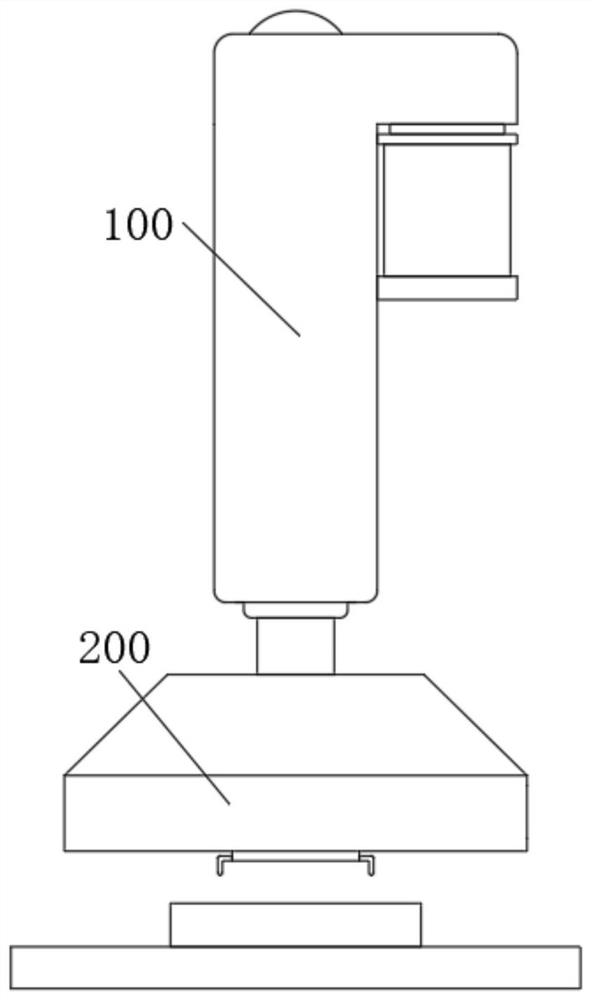
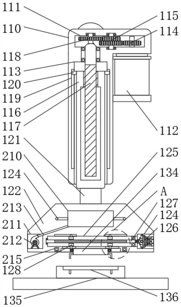
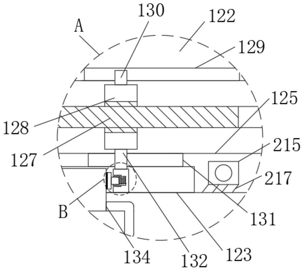
[0028]A semiconductor test chip replacement plug-in device for high efficiency, including a plug-in mechanism 100, a first servo motor 112, a second motor 126 and a blower 212, the plug-in mechanism 100 includes a first shell 110, and the top inside the first shell 110 is opened There is a first transmission chamber 111, the first servo motor 112 is installed on the right end of the f...


PUM


Abstract

The invention relates to the technical field of semiconductor chip testing, in particular to an efficient chip replacing and plugging device for semiconductor testing, which comprises a plugging mechanism, a first servo motor, a second motor and an air blower, a first transmission bin is arranged at the top end in a first shell, and three groups of buffer mechanisms are arranged in a push block. A dust blowing mechanism is arranged in the clamping block, the dust blowing mechanism comprises an air cavity, and a second storage bin is formed in the left end of the clamping block. According to the invention, a large amount of working time is prevented from being wasted when a user installs the semiconductor chip main body, the device can greatly reduce the time of plugging the semiconductor chip main body by the user, the working efficiency of the user is greatly improved, the device has very strong practicability, the influence of dust in the slot on the contact between the slot and the semiconductor chip main body is avoided, and therefore, the safety of the user during testing is improved, and the loss of the user is reduced.

Description

technical field [0001] The invention relates to the technical field of semiconductor chip testing, in particular to an efficient chip replacement plug-in device for semiconductor testing. Background technique [0002] A semiconductor chip is a semiconductor device that can realize a certain function by etching and wiring on a semiconductor sheet. In order to meet the needs of mass production, the electrical properties of semiconductors must be predictable and stable. Therefore, the purity of dopants and the quality of semiconductor lattice structures must be strictly required. Common quality problems include lattice dislocations, Twin planes or stacking faults can affect the properties of semiconductor materials. [0003] When testing a semiconductor chip, the user will plug the semiconductor chip into the testing equipment. Currently, the plugging of some semiconductor chips on the market is not very convenient, and the user wastes the user's working time when plugging, an...

Claims


Application Information

Patent Timeline
Patent Type & Authority Applications(China)
IPC IPC(8): H01R43/26B08B5/02
CPCH01R43/26B08B5/02H01R2201/20
Inventor 吴强
Owner 深圳市瀚鸿创芯科技有限公司
Why Eureka
Try Eureka