LED printing method

A printing method and LED substrate technology, which is applied in printing, printing machines, rotary printing machines, etc., can solve the problems of glue or solder paste not easy to release the mold, low yield, and LED can not be installed normally, so as to avoid glue and solder paste The effect of no demoulding, increasing the success rate, and improving the yield rate of LED printing

Inactive Publication Date: 2021-06-11
SHENZHEN JUFEI OPTOELECTRONICS CO LTD
View PDF16 Cites 1 Cited by
  • Summary
  • Abstract
  • Description
  • Claims
  • Application Information

AI Technical Summary

Problems solved by technology

[0003] The technical problem to be solved by the present invention is that the glue or solder paste is not easy to release the mold during the existing printing screen printing, which leads to the problem that the LED cannot be installed normally and the yield is low. Aiming at this technical problem, a LED printing method is provided, including:

Method used


Image

  • LED printing method
  • LED printing method
  • LED printing method

Examples


no. 1 example

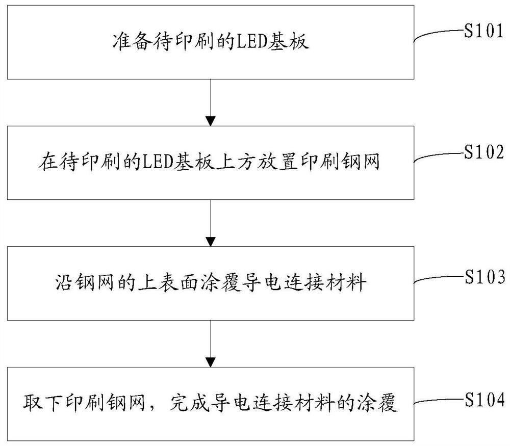
[0029] This embodiment provides a LED printing method, please refer to figure 1 , the method includes:

[0030] S101. Prepare the LED substrate to be printed;

[0031] S102. Place a printing screen above the LED substrate to be printed. The printing screen is a block-shaped flat plate, and there are several via holes penetrating the upper surface and the lower surface of the flat plate, and the aperture of the via hole is along the upper surface of the flat plate to the bottom The direction of the surface gradually increases; the setting position of the via hole corresponds to the pad area on the LED substrate;

[0032] S103, coating the conductive connection material along the upper surface of the printing screen, injecting the conductive connection material into the via hole, and coating it on the corresponding pad area;

[0033] S104. The printing screen is removed, and the coating of the conductive connecting material is completed.

[0034] The characteristic of Mini LE...

no. 2 example

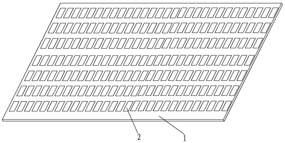
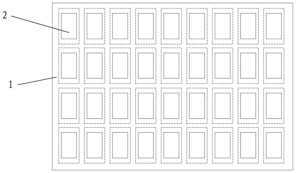
[0049] Please refer to Figure 2-5 , the present embodiment provides a printing screen, which is a block flat plate 1, and the flat plate 1 is provided with several via holes 2 penetrating through the upper surface and the lower surface of the flat plate 1, and the aperture of the via hole 2 is along the upper surface of the flat plate 1. The direction from the surface to the lower surface gradually increases. For the main structure plate 1 of the printing screen, its upper surface is the part where glue or solder paste is injected during the printing process, while the lower surface is the part where glue or solder paste is released. Compared with the upper surface, the lower surface is more close to the substrate. The via hole 2 on the plate 1 is used as a glue injection hole or a solder paste hole, and the size of the hole can be determined according to the bonding point or welding point on the substrate, that is, the pad; due to the characteristics of the via hole 2 in th...


PUM

PropertyMeasurementUnit
sizeaaaaaaaaaa
sizeaaaaaaaaaa

Abstract

The invention provides an LED printing method. The LED printing method comprises the steps: preparing an LED substrate to be printed; placing a printing net above an LED substrate to be printed, wherein the printing net is a blocky flat plate, a plurality of via holes penetrating through the upper surface and the lower surface of the flat plate are formed in the flat plate, and the hole diameters of the via holes are gradually increased in the direction from the upper surface to the lower surface of the flat plate, and the arrangement position of the via hole corresponds to a bonding pad area on the LED substrate; coating a conductive connecting material along the upper surface of the printing net, injecting the conductive connecting material into the via holes, and coating the conductive connecting material on the corresponding bonding pad areas; taking down the printing net, and completing the coating of the conductive connecting material. Therefore, the through holes of the printing screen are set to be big-end-down, the problem that glue and solder paste are not demolded is solved to a great extent, the success rate of LED installation is improved, and the LED printing yield is further improved.

Description

technical field [0001] The invention relates to the field of light-emitting diodes, and more specifically, to an LED printing method. Background technique [0002] With the progress and development of society, the technology of display equipment is constantly innovating, from the backlight display of LCD liquid crystal module, to OLED on the terminal, ultra-small microLED and compromised miniLED, etc. It is the vision of relevant technicians to make the LED module smaller. The smaller the light-emitting unit, the more delicate and accurate the display effect can be. However, due to the small size of the light-emitting unit, correspondingly, it is relatively difficult to inject glue or apply solder paste. During the process of solder paste, the glue or solder paste sticks to the printing screen without releasing the mold, which will further cause the LEDs to fail to form bonding or welding, which directly affects the yield. Contents of the invention [0003] The technical...

Claims


Application Information

Patent Timeline
Patent Type & Authority Applications(China)
IPC IPC(8): H01L33/00H01L33/62
CPCH01L33/005H01L33/62H01L2933/0066H01L33/00B41F15/34
Inventor 陈彦铭孙平如刘永邢美正
Owner SHENZHEN JUFEI OPTOELECTRONICS CO LTD
Why Eureka
Try Eureka