Semiconductor wafer slicing auxiliary device capable of avoiding uneven thickness during slicing

An auxiliary device and semiconductor technology, which is applied to fine working devices, working accessories, stone processing equipment, etc., can solve the problems of uneven thickness of slices, time-consuming and laborious, and inconvenient maintenance, so as to achieve low processing costs, improve work efficiency, and maintain convenient effects

An auxiliary device and semiconductor technology, which is applied to fine working devices, working accessories, stone processing equipment, etc., can solve the problems of uneven thickness of slices, time-consuming and laborious, and inconvenient maintenance, so as to achieve low processing costs, improve work efficiency, and maintain convenient effects

CN112976381AInactive Publication Date: 2021-06-18南京守思商贸有限公司

Image

  • Semiconductor wafer slicing auxiliary device capable of avoiding uneven thickness during slicing
  • Semiconductor wafer slicing auxiliary device capable of avoiding uneven thickness during slicing
  • Semiconductor wafer slicing auxiliary device capable of avoiding uneven thickness during slicing

Examples


Embodiment Construction

[0022] The following will clearly and completely describe the technical solutions in the embodiments of the present invention with reference to the accompanying drawings in the embodiments of the present invention. Obviously, the described embodiments are only some, not all, embodiments of the present invention. Based on the embodiments of the present invention, all other embodiments obtained by persons of ordinary skill in the art without making creative efforts belong to the protection scope of the present invention.

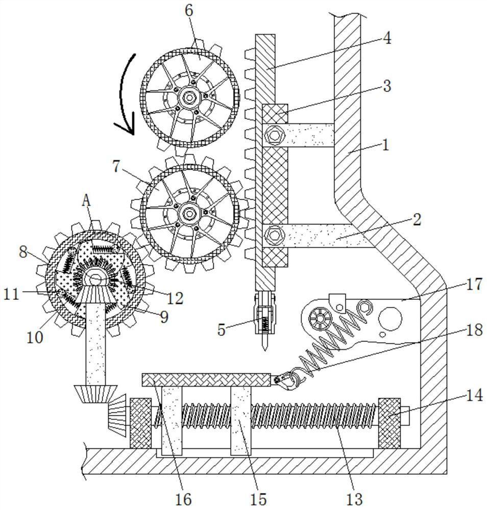
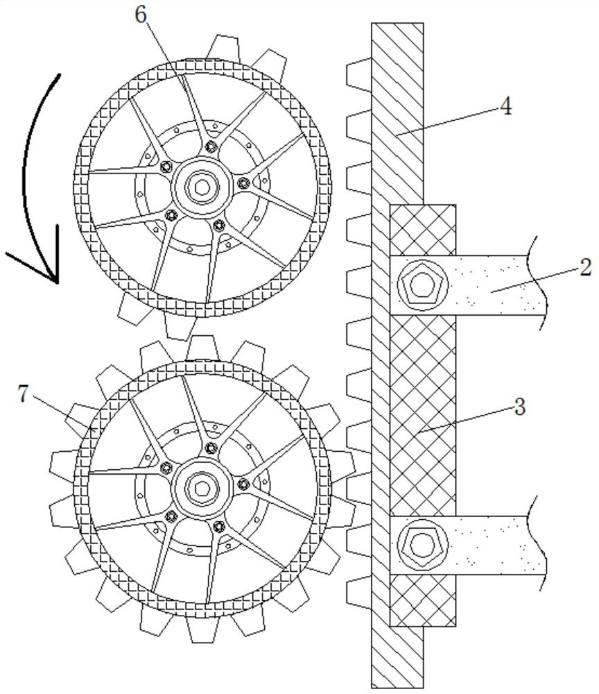
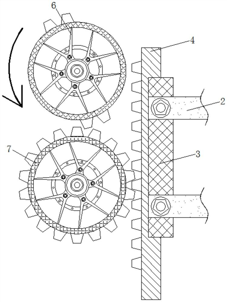
[0023] see Figure 1-4 , an auxiliary device for semiconductor wafer slicing that avoids uneven thickness during slicing, comprising a bracket 1, a mounting column 2 is fixedly installed on the inner wall of the bracket 1, and a slideway 3 is fixedly installed on the end of the mounting column 2 away from the bracket 1, the slideway 3 is slidingly connected with a sliding rack 4 inside, and there are two mounting columns 2, one end is fixedly connected to the ...


PUM


Abstract

The invention relates to the technical field of semiconductor processing equipment, and discloses a semiconductor wafer slicing auxiliary device capable of avoiding uneven thickness during slicing. The semiconductor wafer slicing auxiliary device comprises a support, wherein a mounting column is fixedly mounted on the inner wall of the support, a slide way is fixedly mounted at one end, far away from the support, of the mounting column, and a slide rack is slidably connected in the slide way. According to the semiconductor wafer slicing auxiliary device capable of avoiding uneven thickness during slicing, a driving gear and a sliding rack are driven by a half gear to rotate and move in a reciprocating mode, automatic cutting and lifting of a blade are achieved, meanwhile, a sliding block on the outer side of a threaded rod is driven by a driven gear to move rightwards, equidistant adjustment of wafers is achieved, such that he wafer slicing thickness is more uniform, manual adjustment is not needed, more time and labor are saved, control through a PLC system is not needed, the machining cost is lower, maintenance is more convenient when faults occur, and the working efficiency of equipment is improved to a certain degree.

Description

technical field [0001] The invention relates to the technical field of semiconductor processing equipment, in particular to an auxiliary device for slicing semiconductor wafers that avoids uneven thickness during slicing. Background technique [0002] Semiconductors are used in integrated circuits, consumer electronics, communication systems, photovoltaic power generation, lighting, high-power power conversion and other fields. For example, diodes are devices made of semiconductors. No matter from the perspective of technology or economic development, the importance of semiconductors is huge. Wafers are one of the main materials for semiconductor processing, and the quality of wafers directly affects the performance of semiconductors. [0003] The main processing method of wafers is sheet processing. For the processing of semiconductors with the same specification in the same batch, wafers of the same thickness may be required. Traditional mechanical processing may cause une...

Claims


Application Information

Patent Timeline
18 Jun 2021
Publication
CN112976381A
IPC
B28D5/04; B28D7/04; B28D7/00
CPC
B28D5/0064; B28D5/0082; B28D5/042
Inventors
黄守思