
Photosensitive component manufacturing method, photosensitive component, camera module and mobile terminal

A technology for photosensitive components and manufacturing methods, which can be applied to electrical components, image communications, and parts of color TVs, and can solve problems affecting the yield rate of camera modules, etc.

Pending Publication Date: 2021-06-25
NANCHANG O FILM OPTICAL ELECTRONICS TECH CO LTD
View PDF0 Cites 0 Cited by
  • Summary
  • Abstract
  • Description
  • Claims
  • Application Information

AI Technical Summary

Problems solved by technology

[0004] Based on this, it is necessary to provide a photosensitive component manufacturing method, a photosensitive component, a camera module and a mobile terminal that can improve the yield of the camera module for the problem that the traditional photosensitive component manufacturing method affects the yield rate of the camera module.

Method used


Image

  • Photosensitive component manufacturing method, photosensitive component, camera module and mobile terminal
  • Photosensitive component manufacturing method, photosensitive component, camera module and mobile terminal
  • Photosensitive component manufacturing method, photosensitive component, camera module and mobile terminal

Examples


Embodiment Construction

[0038] In order to make the purpose, technical solution and advantages of the present application clearer, the present application will be further described in detail below in conjunction with the accompanying drawings and embodiments. It should be understood that the specific embodiments described here are only used to explain the present application, and are not intended to limit the present application.

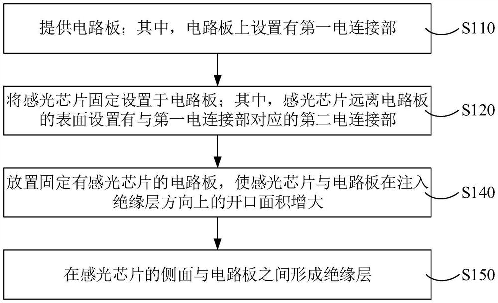
[0039] In one embodiment, a method for making a photosensitive component is provided, such as figure 1 shown, including:

[0040] Step S110: providing a circuit board. Wherein, the circuit board is provided with a first electrical connection part.

[0041] The circuit board is prefabricated, and the first electrical connection part provided on the circuit board is used for electrical connection with other devices. Specifically, the circuit board may be a PCB (Printed Circuit Board, printed circuit board) board or an RPCB (Rigid Printed Circuit Board, rigid printed circu...


PUM


Abstract

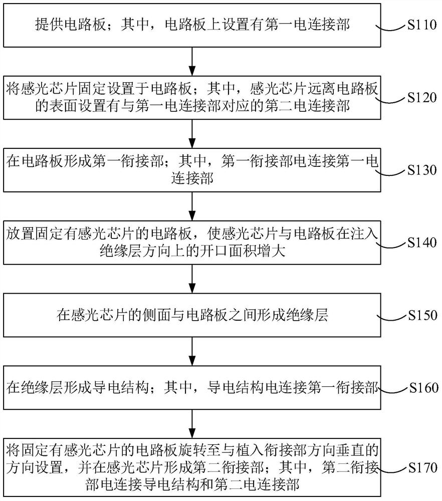
The invention relates to a photosensitive component manufacturing method, a photosensitive component, a camera module and a mobile terminal. The method comprises the following steps: providing a circuit board; arranging a first electric connection part on the circuit board, wherein the photosensitive chip is fixedly arranged on the circuit board, and second electric connection part corresponding to the first electric connection part is arranged on the surface, far away from the circuit board, of the photosensitive chip; placing a circuit board on which a photosensitive chip is fixed, so that the opening area of the photosensitive chip and the circuit board in the direction of injecting the insulating layer is increased; and forming an insulating layer between the side surface of the photosensitive chip and the circuit board, wherein the insulating layer is used for forming a conductive structure electrically connected with the first electric connection part and the second electric connection part. After the photosensitive chip is fixedly arranged on the circuit board, the circuit board on which the photosensitive chip is fixed is placed, so that the opening area of the photosensitive chip and the circuit board in the direction of injecting the insulating layer is increased, the glue is conveniently injected into the glue dispensing needle nozzle to form the insulating layer, the risk of poor electrical connection can be effectively reduced in the subsequent process, and the yield of the camera module is improved.

Description

technical field [0001] The present application relates to the technical field of photography equipment, in particular to a method for manufacturing a photosensitive component, a photosensitive component, a camera module and a mobile terminal. Background technique [0002] A camera module usually includes a photosensitive component and a lens component. The photosensitive component includes a circuit board, a photosensitive chip, and a filter. The board is electrically connected to the pins of the photosensitive chip, and then the photosensitive component and the lens component are packaged together. [0003] The traditional photosensitive component manufacturing method is to install the photosensitive chip on the circuit board, use a needle to fill the insulating material between the photosensitive chip and the welding point on the circuit board, and then form a conductive structure on the insulating material to make the circuit board and photosensitive chip. The pins are e...

Claims


Application Information

Patent Timeline
IPC IPC(8): H04N5/225
CPCH04N23/54
Inventor 罗科朴成炯帅文华
Owner NANCHANG O FILM OPTICAL ELECTRONICS TECH CO LTD
Learn More