Supercharge Your Innovation With Domain-Expert AI Agents!

Overlay test structure, preparation method thereof and overlay test method

A test structure and test method technology, applied in the field of semiconductors, can solve the problem that the boundary signal cannot measure the overlay accuracy normally, and achieve the effects of cost saving, wide application prospect, and simple process optimization.

Active Publication Date: 2021-06-29
CSMC TECH FAB2 CO LTD
View PDF2 Cites 0 Cited by
  • Summary
  • Abstract
  • Description
  • Claims
  • Application Information

AI Technical Summary

Problems solved by technology

[0004] At present, the overlay test structure (OVL mark) has different layers of overlay marks that cannot be detected by the optical lens at the same time. Due to the inability to correctly extract the boundary signal, the overlay accuracy cannot be measured normally.

Method used


Image

  • Overlay test structure, preparation method thereof and overlay test method
  • Overlay test structure, preparation method thereof and overlay test method
  • Overlay test structure, preparation method thereof and overlay test method

Examples


Embodiment 1

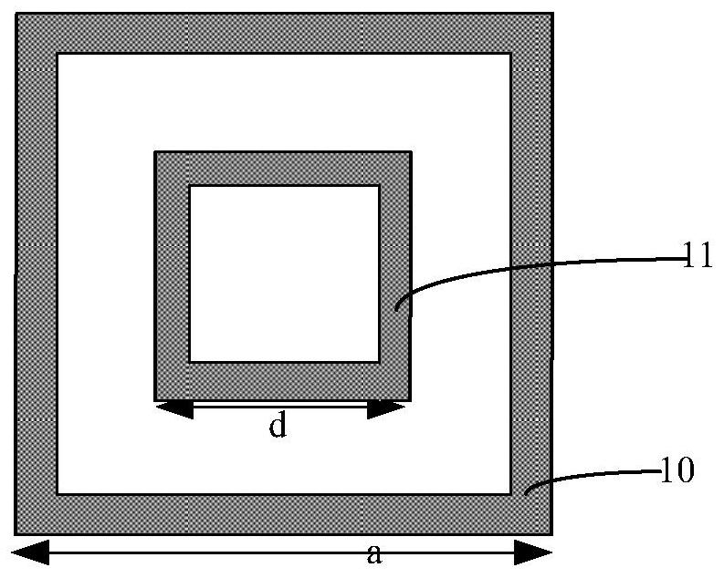
[0077] Attached below Figures 1A-1B ,as well as figure 2 with Figure 4 An overlay alignment standard of the present invention is described in detail. in Figures 1A-1B It shows a schematic top view of an overlay test structure in an embodiment of the present invention; figure 2 It shows a schematic cross-sectional view of an overlay test structure in an embodiment of the present invention; Figure 4 A flowchart showing the steps of a method for preparing an overlay test structure according to an embodiment of the present invention.

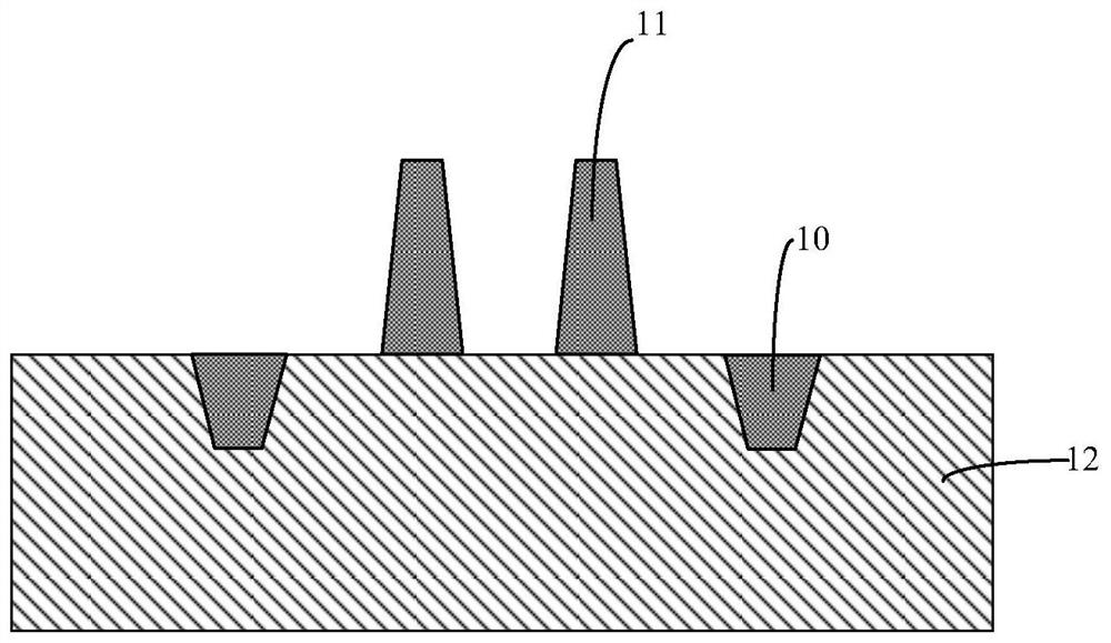
[0078] Such as figure 2 As shown, in this embodiment, the overlay test structure includes:

[0079] base layer 12;

[0080] a first layer of overlay marks 10 formed in the base layer 12;

[0081] The second layer of overlay marks 11 is formed on the first film layer on the base layer, the first layer of overlay marks 10 and the second layer of overlay marks 11 are hollow ring frames and the first layer The size of any border in the rin...

Embodiment 2

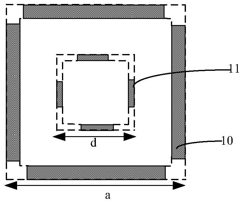
[0124] Attached below Figures 3A-3C ,as well as Figure 5 An overlay test structure of the present invention is described in detail. Figures 3A-3C It shows a schematic cross-sectional view of each device during the preparation process of an overlay test structure in an embodiment of the present invention; Figure 5 A flowchart showing the steps of a method for fabricating a test structure according to another embodiment of the present invention.

[0125] Such as Figure 3C As shown, in this embodiment, the overlay test structure includes:

[0126] base layer 12;

[0127] The first layer of overlay marks 10, formed in the first film layer on the base layer;

[0128] The second overlay mark 11 is formed on the first film layer on the base layer;

[0129] Wherein, the first-layer overlay mark 10 and the second-layer overlay mark 11 are hollow ring frames, and the second-layer overlay mark 11 is arranged on the first-layer overlay mark on the projection of the horizontal p...


PUM

PropertyMeasurementUnit
sizeaaaaaaaaaa
sizeaaaaaaaaaa
thicknessaaaaaaaaaa

Abstract

The invention provides an overlay test structure, a preparation method thereof and an overlay test method. The test structure comprises: a substrate layer; and a first layer of overlay mark and a second layer of overlay mark, wherein the first layer of overlay mark and the second layer of overlay mark are hollow annular frames, the second layer of overlay mark is arranged in the hollow annular frame of the first layer of overlay mark on the projection of the horizontal plane so as to be used for detecting whether the overlay is aligned or not, the first layer of overlay mark is formed in a first film layer on the substrate layer, and the second layer of overlay mark is formed on the first film layer. The problem that automatic focusing fails due to the fact that the total stacking thickness exceeds the range of the simultaneous focusing capacity of the machine table is solved.

Description

technical field [0001] The invention relates to the technical field of semiconductors, in particular to an overlay test structure, a preparation method, and an overlay test method. Background technique [0002] With the rapid development of the electronic industry, higher requirements are put forward for the design and manufacturing process of integrated circuits, such as higher integration, ever-shrinking critical dimension (CD), and multi-functional integration. The photolithography process is the only process for generating patterns in semiconductor manufacturing, and the stability and accuracy of the process directly affects the product yield. Among them, the improvement of the resolution of the projection lithography machine, the control of CD stability and the control of overlay accuracy are always the core issues in the field of lithography. [0003] Since the overlay directly affects the alignment and conduction between the subsequent circuit and the front-layer cir...

Claims


Application Information

Patent Timeline
Patent Type & Authority Applications(China)
IPC IPC(8): G03F9/00G03F1/42G03F1/44H01L23/544
CPCG03F9/708G03F9/7088G03F1/42G03F1/44H01L23/544H01L2223/54426
Inventor 樊航朱福生秦祥
Owner CSMC TECH FAB2 CO LTD
Features
  • R&D
  • Intellectual Property
  • Life Sciences
  • Materials
  • Tech Scout
  • Unparalleled Data Quality
  • Higher Quality Content
  • 60% Fewer Hallucinations
Learn More