CMOS band-gap reference source circuit

A reference source circuit, MOS tube technology, applied in the direction of adjusting electrical variables, control/regulating systems, instruments, etc., can solve the problems of high noise and unstable output, and achieve simple circuit structure, small leakage current, and high signal-to-noise ratio. Effect

Active Publication Date: 2021-06-29
安特(苏州)半导体有限公司
View PDF7 Cites 0 Cited by
  • Summary
  • Abstract
  • Description
  • Claims
  • Application Information

AI Technical Summary

Problems solved by technology

[0004] In view of the above existing problems, the object of the present invention is to provide a CMOS bandgap reference source circuit,

Method used


Image

  • CMOS band-gap reference source circuit

Examples


Embodiment Construction

[0016] The content of the present invention will be described in further detail below in conjunction with the accompanying drawings and specific embodiments.

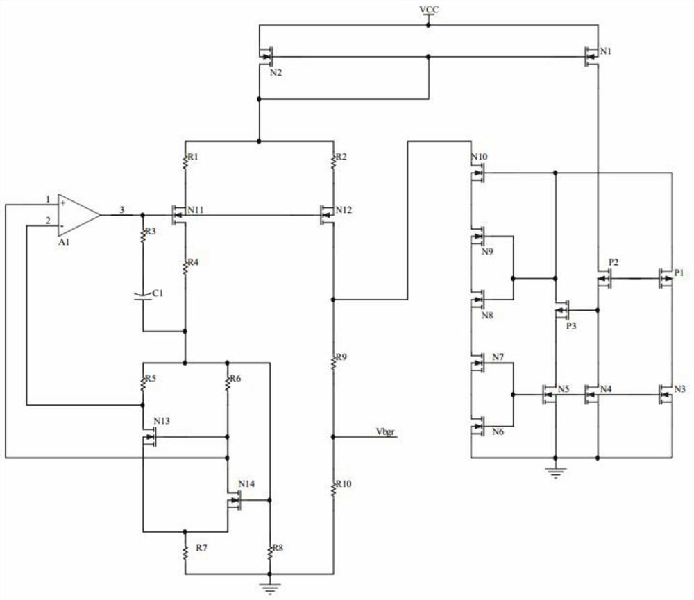
[0017] attached figure 1 As shown, a CMOS bandgap reference source circuit includes a power supply module, a bandgap core circuit, a current source adjustment circuit, the output of the bandgap core circuit is fed back to the current source adjustment circuit, and the current of the current source adjustment circuit is adjusted, and the power supply module The bandgap core circuit is adjusted according to the output of the adjusted current source circuit, and the stable output of the bandgap circuit is realized.

[0018] The circuit has a power supply module composed of MOS transistor N1 and MOS transistor N2, the source of MOS transistor N1 is connected to the source of MOS transistor N2, and connected to the power supply VCC, and the gate of MOS transistor N1 is connected to the gate of MOS transistor N2 , and connec...


PUM


Abstract

The invention provides a CMOS band-gap reference source circuit. The circuit comprises a power supply module, a band-gap core circuit and a current source adjusting circuit, the output of the band-gap core circuit is fed back to the current source adjusting circuit, and the current of the current source adjusting circuit is adjusted. The power supply module adjusts the band-gap core circuit according to the output of the adjusted current source adjusting circuit so that the stable output of the band-gap circuit is realized; and the circuit is provided with a feedback circuit structure, adaptive stable adjustment can be realized, the circuit outputs a stable voltage, and a high integration level, a low noise and a high signal-to-noise ratio of the circuit can be realized through a CMOS device.

Description

technical field [0001] The invention relates to the field of analog integrated circuit design, in particular to a CMOS bandgap reference source circuit. Background technique [0002] The current development of electronic technology tends to be miniaturized and integrated, especially the latest wearable devices, whose product size is getting smaller and smaller, which requires higher and higher requirements for circuit design. On the one hand The size of the circuit needs to be small enough, and on the other hand, the stability of the circuit needs to be high enough; and the power supply circuit is the most commonly used analog circuit in electronic circuits. The smaller the device, the more stable power supply circuit is needed to ensure the stable operation of the circuit. [0003] Due to the small size of wearable device products, it is more susceptible to the influence of the external environment, and the increase in the degree of circuit integration is interfered by oth...

Claims


Application Information

Patent Timeline
IPC IPC(8): G05F1/56
CPCG05F1/56
Inventor 陈强张艳波姚罗燕
Owner 安特(苏州)半导体有限公司
Why Eureka
Try Eureka