
Light-emitting panel, preparation method thereof and light-emitting device

A technology for light-emitting panels and light-emitting areas, which is applied in the manufacturing of semiconductor/solid-state devices, semiconductor devices, electrical components, etc., can solve problems such as poor isolation effect, and achieve the effect of increasing the barrier effect, weakening the climbing ability, and improving reliability.

Pending Publication Date: 2021-07-02
HEFEI XINSHENG OPTOELECTRONICS TECH CO LTD +1
View PDF3 Cites 2 Cited by
  • Summary
  • Abstract
  • Description
  • Claims
  • Application Information

AI Technical Summary

Problems solved by technology

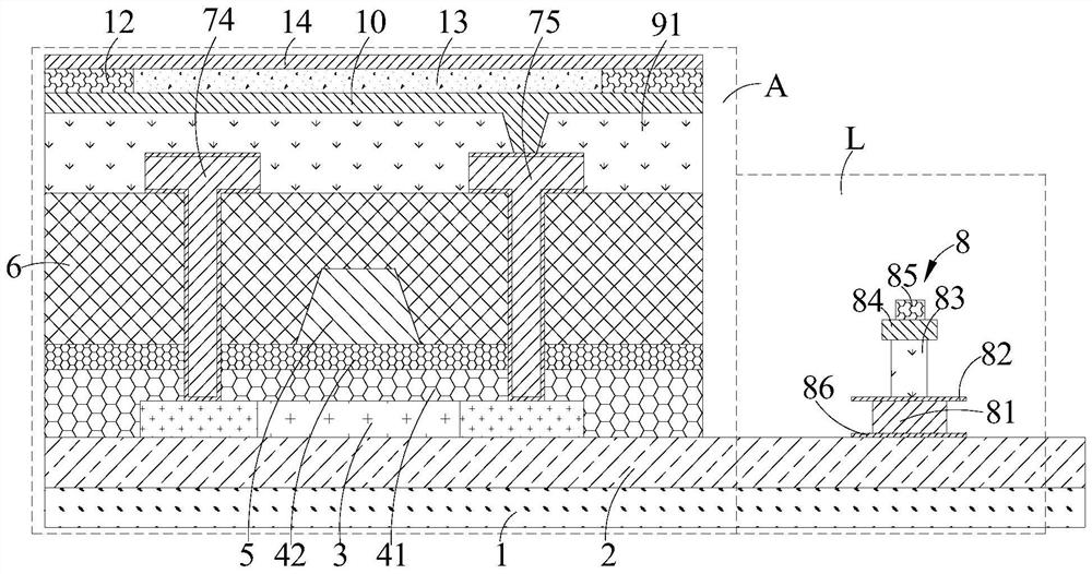
[0004] The purpose of the present disclosure is to overcome the disadvantages of the poor isolation effect of the prior art, and provide a light-emitting panel with a better isolation effect, a method for preparing the light-emitting panel, and a light-emitting device including the light-emitting panel.

Method used


Image

  • Light-emitting panel, preparation method thereof and light-emitting device
  • Light-emitting panel, preparation method thereof and light-emitting device
  • Light-emitting panel, preparation method thereof and light-emitting device

Examples


Embodiment Construction

[0056] Example embodiments will now be described more fully with reference to the accompanying drawings. Example embodiments may, however, be embodied in many forms and should not be construed as limited to the embodiments set forth herein; rather, these embodiments are provided so that this disclosure will be thorough and complete, and will fully convey the concept of example embodiments to those skilled in the art. The same reference numerals in the drawings denote the same or similar structures, and thus their detailed descriptions will be omitted. Furthermore, the drawings are merely schematic illustrations of the present disclosure and are not necessarily drawn to scale.

[0057] Although relative terms such as "upper" and "lower" are used in this specification to describe the relative relationship of one component of an icon to another component, these terms are used in this specification only for convenience, for example, according to the description in the accompanyin...


PUM

PropertyMeasurementUnit
thicknessaaaaaaaaaa
thicknessaaaaaaaaaa
thicknessaaaaaaaaaa

Abstract

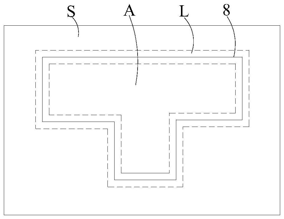
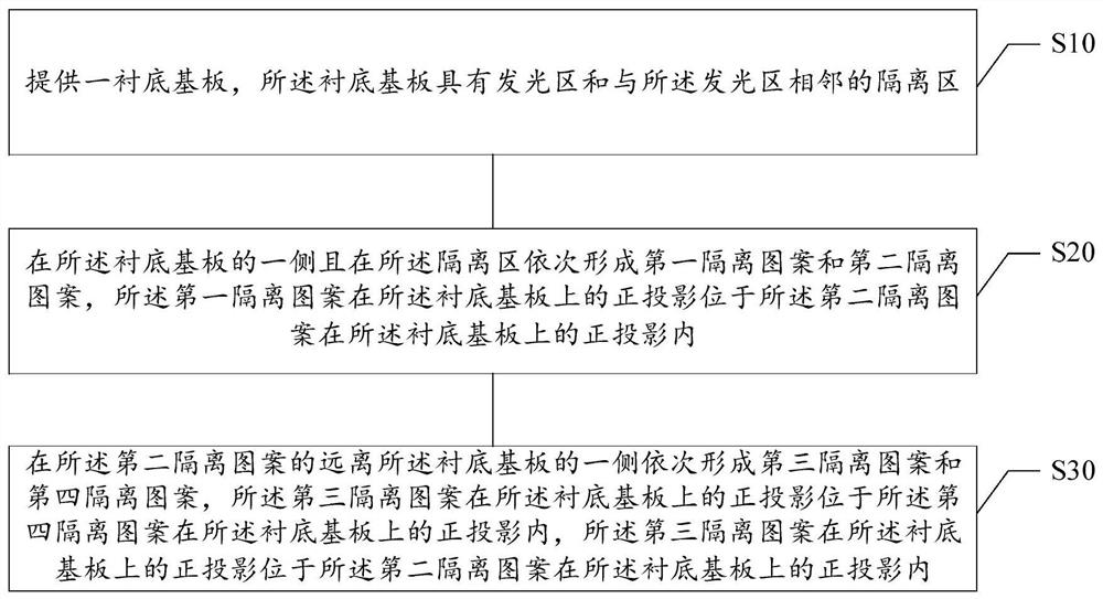
The invention relates to the technical field of illumination and display, and discloses a light-emitting panel, a preparation method thereof and a light-emitting device. The light-emitting panel is provided with a light-emitting area and an isolation area adjacent to the light-emitting area. The light-emitting panel comprises a substrate and a barrier structure. The barrier structure is arranged on one side of the substrate and located in the isolation region and comprises a first isolation pattern, a second isolation pattern, a third isolation pattern and a fourth isolation pattern which are sequentially stacked, and the first isolation pattern is closer to the substrate than the fourth isolation pattern; the orthographic projection of the first isolation pattern on the substrate is located in the orthographic projection of the second isolation pattern on the substrate, and the orthographic projection of the third isolation pattern on the substrate is located in the orthographic projection of the fourth isolation pattern on the substrate. The orthographic projection of the third isolation pattern on the substrate is located in the orthographic projection of the second isolation pattern on the substrate. The blocking structure of the light-emitting panel forms a double-layer I-shaped structure, and the blocking effect is good.

Description

technical field [0001] The present disclosure relates to the technical field of lighting and display, and in particular, to a light-emitting panel, a method for preparing the light-emitting panel, and a light-emitting device including the light-emitting panel. Background technique [0002] With more and more requirements for special-shaped light emission, the shape of the light-emitting area is different from the regular rectangular light-emitting area. It is necessary to design the isolation part to block and isolate the light-emitting functional layer and the cathode to achieve light emission in the special-shaped area; however, the current isolation part The isolation effect is not ideal. [0003] It should be noted that the information disclosed in the above background section is only for enhancing the understanding of the background of the present disclosure, and therefore may include information that does not constitute the prior art known to those of ordinary skill in...

Claims


Application Information

Patent Timeline
Patent Type & Authority Applications(China)
IPC IPC(8): H01L27/32H01L51/52H01L51/56
CPCH10K59/12H10K50/84H10K71/00H10K59/873H10K59/1213H10K59/124H10K59/122H10K59/8051H10K59/1201
Inventor 刘军汪军刘宁苏同上王海东周斌桂学海刘融
Owner HEFEI XINSHENG OPTOELECTRONICS TECH CO LTD
Learn More