Resistive random-access memory device and manufacturing method thereof

A resistive storage and variable technology, applied in information storage, static storage, digital storage information, etc., can solve the problems of difficult manufacturing engineering, decreased yield, and increased manufacturing cost.

Active Publication Date: 2021-07-06
WINBOND ELECTRONICS CORP
View PDF6 Cites 0 Cited by
  • Summary
  • Abstract
  • Description
  • Claims
  • Application Information

AI Technical Summary

Problems solved by technology

However, the manufacturing engineering for this is not easy, which may lead to increased manufacturing costs or lower yields

Method used


Image

  • Resistive random-access memory device and manufacturing method thereof
  • Resistive random-access memory device and manufacturing method thereof
  • Resistive random-access memory device and manufacturing method thereof

Examples


Embodiment Construction

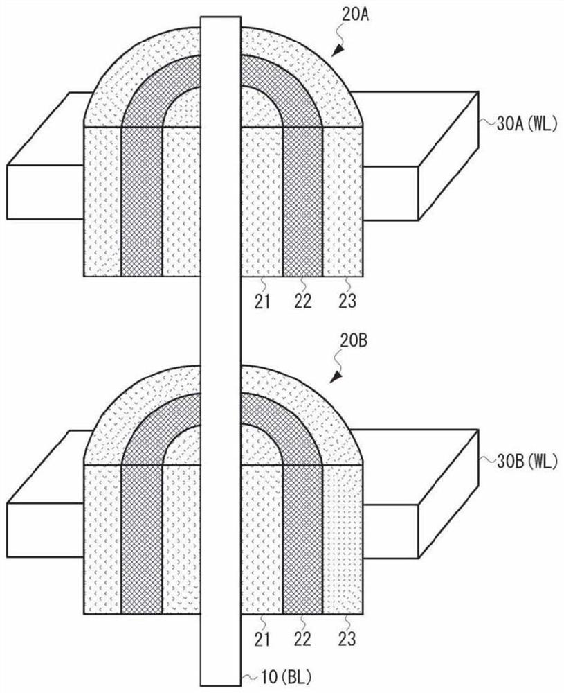
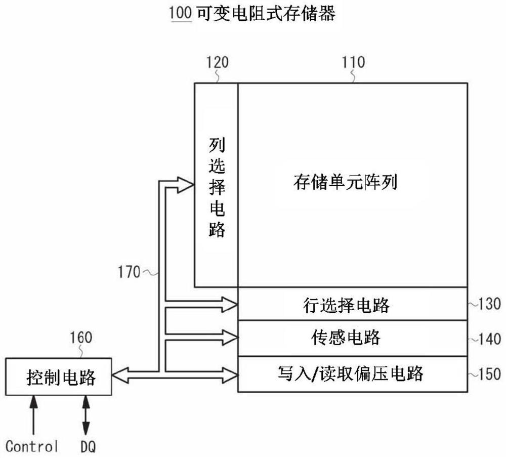
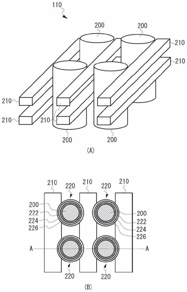
[0061] The present invention provides a variable resistance memory including a stacked memory cell array (ie, a memory cell array having a three-dimensional structure). The variable resistance memory of the present invention not only has the function of randomly accessing memory cells, but also has the function of simultaneously accessing multiple memory cells. A memory cell formed in a three-dimensional structure includes an access transistor between a pair of bit lines, and variable resistance elements formed on both sides thereof. For the memory cells in the column direction, the bit line is shared between adjacent memory cells, and the memory cells are selected so that when the memory cells on one side are selected, the memory cells on the other side are unselected, preventing the selection of connection selection memory cells On the bit line, an undesired sneak path is formed.

[0062] In addition, the three-dimensional memory cell array of the present invention can be a...


PUM


Abstract

The invention provides a resistive random-access memory device and a manufacturing method thereof. The resistive random-access memory includes a plurality of pillars, a plurality of bit lines, and a memory cell. The pillars extend vertically along the main surface of the substrate. The bit lines extend in a horizontal direction. The memory cell is formed at the intersection of the pillars and the bit lines. The memory cell includes a gate insulating film, a semiconductor film, and a resistive element. The gate insulating film is formed on the circumference of the pillar. The semiconductor film is formed on the circumference of gate insulating film and provides a channel area. The resistive element is formed on the circumference of the semiconductor film. A first electrode area on the circumference of the resistive element and a second electrode area facing the first electrode area are electrically connected to a pair of adjacent bit lines.

Description

technical field [0001] The present invention relates to a variable resistance memory device using a variable resistance memory cell, and more particularly to a three-dimensional configuration of an array including a variable resistance memory cell. Background technique [0002] Variable resistance random access memory (hereinafter referred to as "variable resistance memory") can randomly select memory cells according to the column address and row address, read data from the selected memory cell, or write data into the selected storage unit. In order to achieve a high degree of integration, the technology of manufacturing variable resistive memory with a three-dimensional structure has been disclosed in patent literature (US Patent Application Publication No. 2017 / 0330916 ), for example. patent literature for variable resistive memories, such as figure 1 As shown, it includes: pillars 10 extending along the vertical direction as bit lines; word lines 30A, 30B extending alon...

Claims


Application Information

Patent Timeline
Patent Type & Authority Applications(China)
IPC IPC(8): H01L27/24H01L45/00
CPCH10B63/80H10B63/84H10N70/801H10N70/011G11C13/003G11C13/004G11C13/0069G11C13/0026G11C13/0028G11C2213/52G11C2213/18G11C2213/79G11C2213/71G11C2213/78H10B63/30H10N70/20H10N70/823H10N70/8833H10N70/821H10N70/841H10N70/826G11C2213/75G11C13/0007H10B63/845H10B63/34H10N70/24H10N70/066
Inventor 矢野胜
Owner WINBOND ELECTRONICS CORP
Why Eureka
Try Eureka