LCD panel, its manufacture method and LCD device using the same

A liquid crystal display panel, panel technology, applied in static indicators, nonlinear optics, instruments, etc., can solve the problems of complex driving voltage waveform and driving circuit, low yield, etc., to improve the viewing angle characteristics, simplify manufacturing engineering, The effect of increasing the elastic space

Active Publication Date: 2009-07-01
AU OPTRONICS CORP
View PDF6 Cites 0 Cited by
  • Summary
  • Abstract
  • Description
  • Claims
  • Application Information

AI Technical Summary

Problems solved by technology

[0007] The first method is the pixel area segmentation method, and its disadvantage is that the more sub-pixels are divided, the lower the production yield (yield) will be.
[0008] The second method is the picture time division method, and its disadvantage is that a high-speed driving circuit is required to cut the gray scale.
[0009] The third method is the driving voltage division method. The disadvantage is that the liquid crystal display panel with photoelectric bistable characteristics is driven by the voltage, and the driving voltage waveform and the driving circuit become very complicated.

Method used


Image

  • LCD panel, its manufacture method and LCD device using the same
  • LCD panel, its manufacture method and LCD device using the same
  • LCD panel, its manufacture method and LCD device using the same

Examples


Embodiment 1

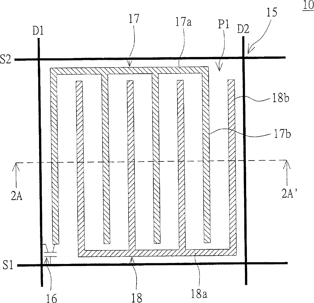
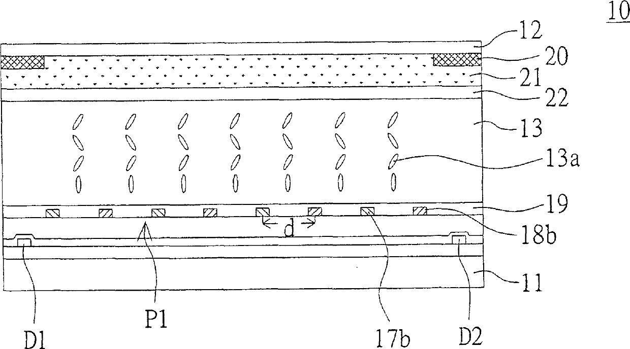
[0055] Please also refer to Figures 1 to 2A , figure 1 A schematic top view showing the circuit structure of the liquid crystal display panel according to the first embodiment of the present invention, Figure 2A Draw along figure 1 A schematic diagram of a partial cross-sectional structure of the liquid crystal display panel viewed from the section line 2A-2A'. exist Figures 1 to 2A The liquid crystal display panel 10 includes an active matrix 15 , a first electrode 17 , a second electrode 18 , a first vertical alignment film 19 , a second vertical alignment film 22 and a smectic liquid crystal layer 13 . The active matrix 15 has one or more switch elements and one or more pixels, and is disposed on the first substrate 11 . Each pixel is defined by the interval between two adjacent scan lines (or gate lines) and two adjacent data lines (or source lines) disposed on the first substrate 11 . In this embodiment, the active matrix 15 is illustrated by taking the pixel P1 a...

Embodiment 2

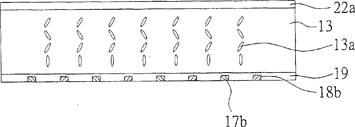
[0078] Please also refer to 8A to 8B , which shows a schematic diagram of a partial cross-sectional structure of the liquid crystal display panel according to the second embodiment of the present invention. The difference between the liquid crystal display panels 10 a to 10 b of the present embodiment and the liquid crystal display panel 10 of the first embodiment is that there is only a vertical alignment film. As for other identical constituent elements, the reference numerals will continue to be used, and will not be repeated.

[0079] like Figure 8AAs shown, the liquid crystal display panel 10a has only the first vertical alignment film 19 with strong anchoring energy, but does not have the second vertical alignment film 22, so that the anchoring energy provided by the second substrate 12 relative to the smectic liquid crystal layer 13 is almost Zero, not even. Therefore, the layer of liquid crystal molecules 13a of the smectic liquid crystal layer 13 adjacent to the ...

Embodiment 3

[0086] Please refer to Figure 10 , which shows a schematic diagram of a partial cross-sectional structure of the liquid crystal display panel according to the third embodiment of the present invention. The difference between the liquid crystal display panel 40 of the present embodiment and the liquid crystal display panel 10 of the first embodiment lies in the position of the color filter 41 . The rest of the same constituent elements continue to use the labels, and will not be repeated.

[0087] like Figure 10 As shown, the color filter 41 is disposed between the first substrate 11 and the first vertical alignment film 19 . In this embodiment, the color filter 41 covers the first electrode 17 and the second electrode 18 , here Figure 10 Only the color filter 41 is shown covering the first electrode portion 17 b of the first electrode 17 and the second electrode portion 18 b of the second electrode 18 . The first vertical alignment film 19 covers the color filter 41 . ...


PUM


Abstract

The invention discloses a liquid crystal display panel, which comprises an active matrix, a first electrode, a second electrode, a first vertical alignment film, a second vertical alignment film and a layer of liquid crystal layers. The first electrode has a plurality of first electrode parts. The second electrode has a plurality of second electrode parts, and the second electrode parts are arranged in parallel with the first electrode parts at a predetermined interval. By applying an AC voltage to the first and second electrodes, the direction of the transverse electric field formed by any adjacent first electrode portion and second electrode portion is parallel to the surface of the first substrate. The first vertical alignment film is disposed on the first substrate and covers the first and second electrodes. The second vertical alignment film is disposed on the second substrate. The smectic liquid crystal layer is disposed between the first and second substrates. During the phase transition process of the liquid crystal molecules in the smectic liquid crystal layer, the transverse electric field generated by applying the AC voltage to the first and second electrodes assists the alignment of the liquid crystal molecules in the smectic liquid crystal layer.

Description

technical field [0001] The present invention relates to a liquid crystal display panel, a method for manufacturing the same, and a liquid crystal display device using the same, and in particular, to a liquid crystal molecule alignment in the smectic liquid crystal layer using an alternating voltage during the phase transition process of the liquid crystal molecules in the smectic liquid crystal layer, and A liquid crystal display panel adopting the design of vertical alignment of liquid crystal, a manufacturing method thereof, and a liquid crystal display device using the same. Background technique [0002] In a conventional ferroelectric liquid crystal (FLC) display panel, the alignment of its smectic liquid crystal layer is performed using a hard rubbing method. Therefore, the alignment defect of the zig-zag wall (Zig-Zag Wall) is easily generated in the alignment of the liquid crystal of the conventional smectic liquid crystal layer. As a result, the conventional FLC dis...

Claims


Application Information

Patent Timeline
Patent Type & Authority Patents(China)
IPC IPC(8): G02F1/136G02F1/1337G02F1/133G02F1/1335G02F1/1333
Inventor 林子原刘埃森黄仁宏吴柏昌谢富程姜俊宏吴勋隆吴俊杰陈伯纶
Owner AU OPTRONICS CORP
Why Eureka
Try Eureka