
Semiconductor package

A semiconductor and external conduction technology, applied in the direction of semiconductor devices, semiconductor/solid-state device components, electric solid-state devices, etc., can solve problems such as power consumption, and achieve the effect of short conductive path, fast signal transmission, and shortened connection path.

Pending Publication Date: 2021-07-20
MEDIATEK INC
View PDF0 Cites 0 Cited by
  • Summary
  • Abstract
  • Description
  • Claims
  • Application Information

AI Technical Summary

Problems solved by technology

[0002] Passive components are those that do not generate electricity, but consume, store and / or release electricity

Method used


Image

  • Semiconductor package
  • Semiconductor package
  • Semiconductor package

Examples


Embodiment Construction

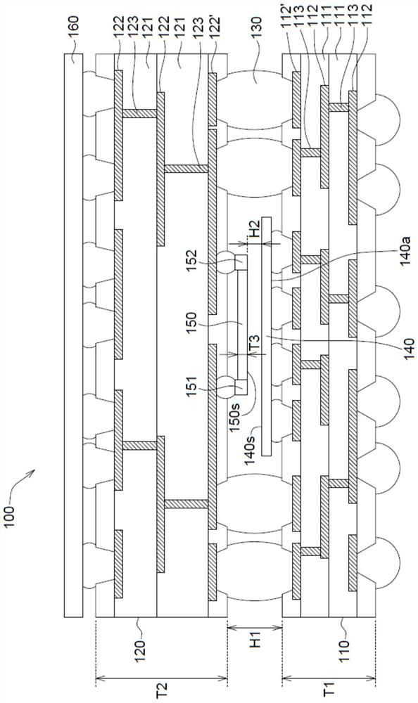
[0022] refer to figure 1 , figure 1 A schematic diagram of a semiconductor package 100 according to an embodiment of the present invention is shown. The semiconductor package 100 may be applied to electronic devices such as mobile phones, laptop computers, tablet computers, desktop computers, and the like. The semiconductor package is, for example, a PoP (Package-On-Package, package-on-package) structure.

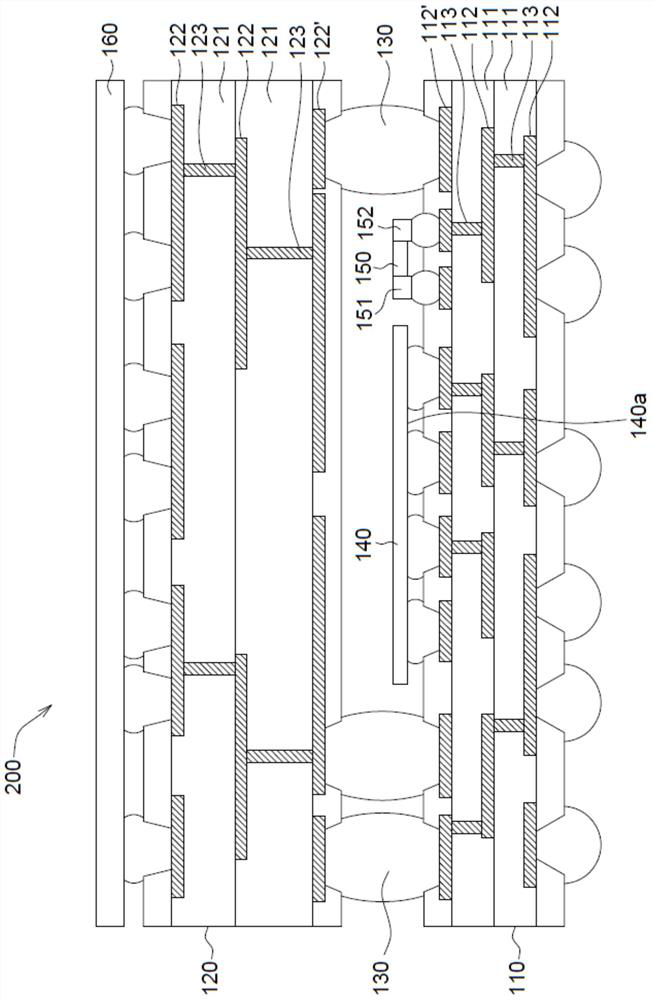
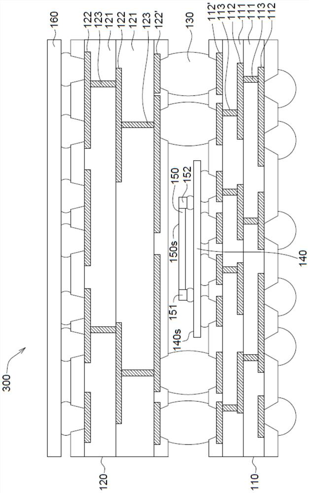
[0023] The semiconductor package 100 includes a first substrate 110 , a second substrate 120 , at least one conductive component 130 , at least one electronic component 140 and at least one passive component 150 . The conductive member 130 is disposed between the first substrate 110 and the second substrate 120, and the first substrate 110 and the second substrate 120 are separated from each other by an interval H1. Both the electronic part 140 and the passive part 150 are disposed within the interval H1. Therefore, the electronic component 140 and the passive component...


PUM

PropertyMeasurementUnit
thicknessaaaaaaaaaa

Abstract

A semiconductor package includes a first substrate, a second substrate, a conductive component, an electronic component and a passive component. The conductive component is disposed between the first substrate and the second substrate, and the first substrate and the second substrate are separated from each other by an interval. The electronic component and the passive component are disposed within the interval. In this way, a conductive path between the electronic component and the passive component is shorter, a connection path between the electronic component and the passive component can be shortened, and signal transmission is faster.

Description

technical field [0001] The invention relates to the technical field of semiconductors, in particular to a semiconductor package. Background technique [0002] A passive component is one that does not generate electricity, but consumes, stores, and / or releases electricity. Passive components include resistors, capacitors and inductors. In most circuits, passive components are connected to active components, usually semiconductor devices such as amplifiers and logic chips. [0003] Therefore, how to connect with semiconductor devices to increase transmission speed has become an important task in industry. Contents of the invention [0004] In view of this, the present invention provides a semiconductor package to solve the above problems. [0005] According to a first aspect of the present invention, a semiconductor package is disclosed, comprising: [0006] first substrate; [0007] second substrate; [0008] a conductive component disposed between the first substrate...

Claims


Application Information

Patent Timeline
Patent Type & Authority Applications(China)
IPC IPC(8): H01L23/31H01L23/488
CPCH01L23/3128H01L24/02H01L24/13H01L2224/02331H01L2224/02333H01L2224/02381H01L2224/02379H01L2224/13008H01L2924/15331H01L2924/19105H01L2924/19104H01L2224/16237H01L2224/16265H01L2224/17181H01L25/16H01L25/105H01L2225/1023H01L2225/1058H01L2924/19103H01L2224/1703H01L2924/1434H01L2224/73253H01L2924/1431H01L2924/19041H01L2924/19042H01L2924/19043H01L24/16H01L2224/32265H01L23/5385H01L23/5386H01L25/162
Inventor 吕添裕胡楚威萧欣欣
Owner MEDIATEK INC
Learn More