Insulated Gate Bipolar Transistor, Power Module, and Living Appliance

a technology of insulated gate bipolar transistor and power module, which is applied in the direction of basic electric elements, electrical equipment, and semiconductor devices, can solve the problems of higher conduction loss generated by igbt, and achieve the effect of reducing the effective thickness of the drift region, reducing the overall conduction loss, and reducing the conduction loss

Pending Publication Date: 2022-07-28
GUANGDONG MIDEA WHITE HOME APPLIANCE TECH INNOVATION CENT CO LTD +1
View PDF0 Cites 0 Cited by
  • Summary
  • Abstract
  • Description
  • Claims
  • Application Information

AI Technical Summary

Benefits of technology

[0016]According to the present disclosure, the insulated gate bipolar transistor has a collector region that is doped in a first type. The collector region includes a bump region. The insulated gate bipolar transistor has a drift region that is doped in a second type. The drift region locates on a side of the collector region and includes a first drift region and a second drift region. The first drift region has a higher doping concentration, directly contacts the bump region, and has a profile matching the bump region, such that the second drift region that has a lower doping concentration does not contact the bump region. While the IGBT is conducted, channels in a first active region and a second active region are unblocked. Due to presence of the bumped region, an effective thickness of the drift region is reduced, and electrons (or holes) from the first active region and the second active region and the holes (or electrons) from the collector region may flow through a shorter conduction path, accelerating electron-hole complex, reducing the conduction loss in the drift region, thus reducing an overall conduction loss of the IGBT. Further, since the first active region and the second active region are formed at two ends of the second drift region that has the lower doping concentration, a voltage withstand range of the IGBT is larger and a voltage withstand capability is better.

Problems solved by technology

The higher the conduction resistance, the higher the conduction loss is generated while the IGBT is operating.

Method used


Image

  • Insulated Gate Bipolar Transistor, Power Module, and Living Appliance
  • Insulated Gate Bipolar Transistor, Power Module, and Living Appliance
  • Insulated Gate Bipolar Transistor, Power Module, and Living Appliance

Examples


Embodiment Construction

[0025]Technical solutions in the embodiments of the present disclosure will be clearly and completely described by referring to the accompanying drawings in the embodiments of the present disclosure. Apparently, the embodiments described are only a part of, but not all of, the embodiments of the present disclosure. All other embodiments that are obtained by an ordinary skilled person in the art based on the embodiments of the present disclosure without making creative work shall fall within the scope of the present disclosure.

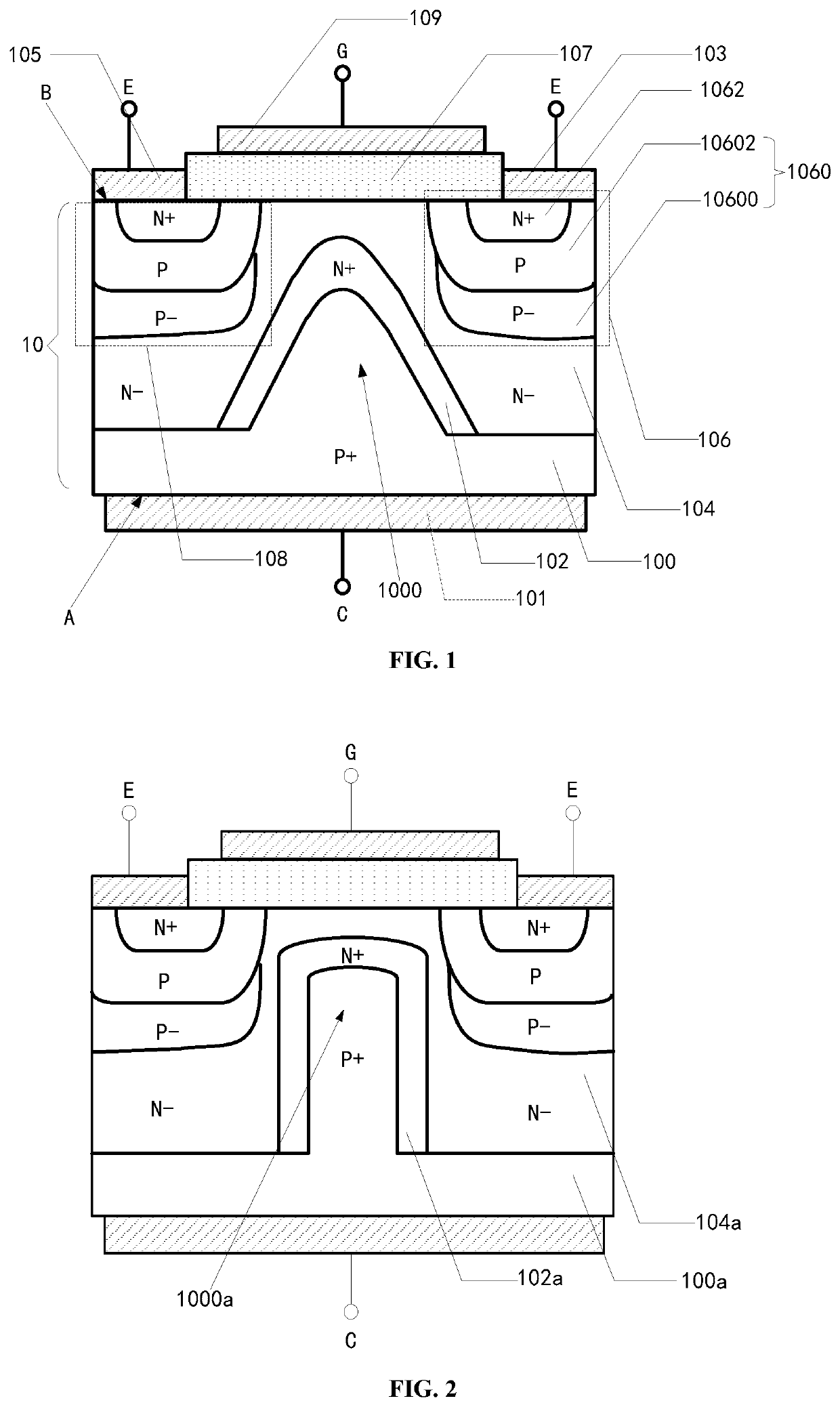
[0026]As shown in FIG. 1, FIG. 1 is a structural schematic view of an IGBT according to some embodiments of the present disclosure. The IGBT includes a semiconductor substrate 10, which may be made of silicon, silicon carbide, germanium, silicon germanium crystals, gallium nitride, gallium arsenide, and so on. The IGBT may be cube-shaped and the like. The semiconductor substrate 10 includes a collector region 100 that is doped in a first type, a first drift reg...


PUM

PropertyMeasurementUnit
doping concentrationaaaaaaaaaa
thicknessaaaaaaaaaa
voltagesaaaaaaaaaa

Abstract

An insulated gate bipolar transistor includes a semiconductor substrate, and the semiconductor substrate includes: a collector region doped in a first type, wherein the collector region includes a bump region; a first drift region doped in a second type and a second drift region doped in the second type; wherein the first drift region and the second drift region locate on a side of the collector region having the bump region, a profile contour of the first drift region matches a profile contour of the bump region, such that the second drift region does not contact the bump region, and a doping concentration of the first drift region is greater than a doping concentration of the second drift region; and a first active region and a second active region, formed at two opposite ends of the second drift region.

Description

CROSS REFERENCE TO RELATED APPLICATIONS[0001]The present application is a continuation application of International (PCT) Patent Application No. PCT / CN2019 / 125921, filed on Dec. 17, 2019, which claims the priority of Chinese Patent Application No. 201911013226.4, filed on Oct. 23, 2019, in the title of “INSULATED GATE BIPOLAR TRANSISTOR, POWER MODULE, AND LIVING APPLIANCE”, in China National Intellectual Property Administration, the entire contents of which are hereby incorporated by reference in their entireties.TECHNICAL FIELD[0002]The present disclosure relates to the field of power electronics, and in particular to an insulated gate bipolar transistor, a power module and an electrical appliance.BACKGROUND[0003]An insulated gate bipolar transistor (IGBT) is a power semiconductor device, which consists of a bipolar triode and an insulated gate field effect tube and is a composite all-control device driven by voltages. Since the IGBT has a high input impedance, a low conduction vol...

Claims


Application Information

Patent Timeline
Patent Type & Authority Applications(United States)
IPC IPC(8): H01L29/739H01L29/10
CPCH01L29/7395H01L29/1095H01L29/0619H01L29/0821H01L29/7397H01L29/0834
Inventor LIU, LISHUFENG, YUXIANG
Owner GUANGDONG MIDEA WHITE HOME APPLIANCE TECH INNOVATION CENT CO LTD
Why Eureka
Try Eureka