Manufacture method of wafer level upright type diode packaging structure

A technology of packaging structure and manufacturing method, applied in semiconductor/solid-state device manufacturing, electrical components, electrical solid-state devices, etc., can solve the problems of increased material cost, processing cost, poor electrical conductivity, long electrical path, etc., to reduce material cost, The effect of good electrical conductivity and short electrical path

Active Publication Date: 2012-05-30
HARVATEK CORPORATION
View PDF0 Cites 0 Cited by
  • Summary
  • Abstract
  • Description
  • Claims
  • Application Information

AI Technical Summary

Problems solved by technology

[0004] 1. Since the known diode packaging structure still requires two manufacturing processes of "metal bonding" and "colloid packaging", this results in an increase in "material cost" and "processing cost"
[0005] 2. Since the known diode packaging structure still needs to generate a conductive connection with the circuit board D through the metal wire L, the conductive path of the known diode packaging structure is relatively long and has poor conductivity
[0006] Therefore, it can be seen from the above that the above-mentioned known diode packaging structure obviously has inconvenience and technical defects in actual use.

Method used


Image

  • Manufacture method of wafer level upright type diode packaging structure
  • Manufacture method of wafer level upright type diode packaging structure
  • Manufacture method of wafer level upright type diode packaging structure

Examples


Embodiment Construction

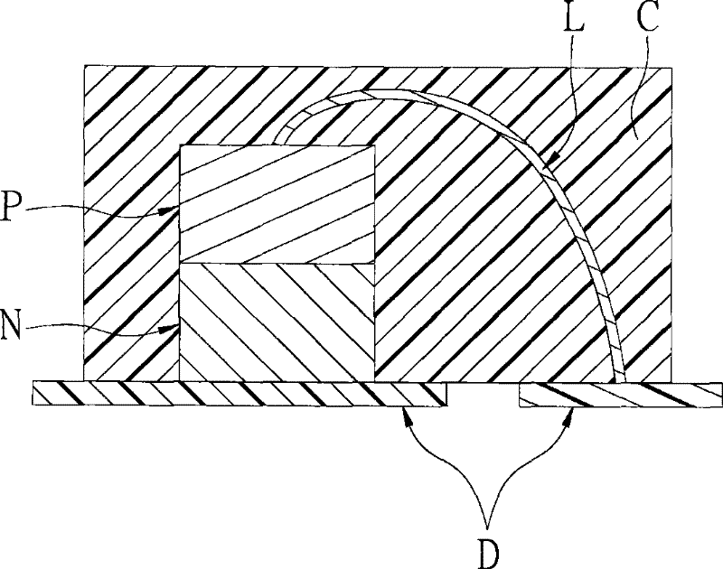
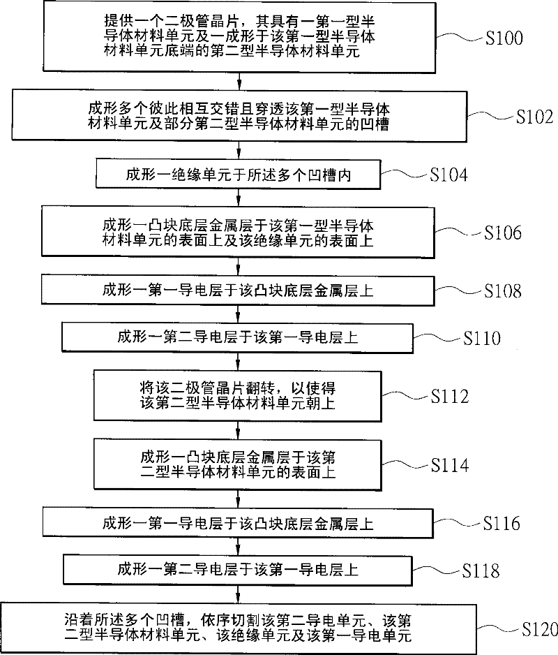
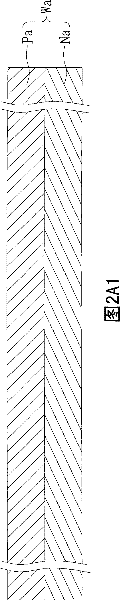
[0104] see figure 2 , Figure 2A1 to Figure 2I1 ,and Figure 2I2 shown, where figure 2 It is a flow chart of the first embodiment of the manufacturing method of the wafer-level vertical diode packaging structure of the present invention; Figure 2A1 to Figure 2I1 It is a schematic cross-sectional view of the manufacturing process of the first embodiment of the manufacturing method of the wafer-level vertical diode packaging structure of the present invention; Figure 2I2 It is a three-dimensional schematic view of the first embodiment of the wafer-level vertical diode packaging structure of the present invention. It can be seen from the above-mentioned figures that the first embodiment of the present invention provides a method for manufacturing a wafer-level vertical diode packaging structure, which includes the following steps:

[0105] Step S100 is: first, coordinate figure 2 , Figure 2A1 and Figure 2A2 shown (where Figure 2A1 for Figure 2A2 Partial cross-se...


PUM


Abstract

The invention relates to a manufacture method of a wafer level upright type diode packaging structure. The diode packaging structure comprises a semiconductor material layer I, a semiconductor material layer II, an insulating unit, a first conducting structure and a second conducting structure, wherein the semiconductor material layer II is connected to one surface of the semiconductor material layer I; the insulating unit is coated at the peripheries of the semiconductor material layer I and the semiconductor material layer II; the first conducting structure is formed on the surface of the semiconductor material layer I and one side edge of the insulating unit; and the second conducting structure is formed on the surface of the semiconductor material layer II and the other opposite side edge of the insulating unit. The semiconductor material layer I and the semiconductor material layer II are completely coated by the insulating unit, the first conducting structure and the second conducting structure. The invention reduces the material cost and the processing cost; and the diode packaging structure has shorter conducting path and better conducting characteristic.

Description

technical field [0001] The invention relates to a method for manufacturing a diode packaging structure, in particular to a method for manufacturing a wafer-level vertical diode packaging structure. Background technique [0002] see figure 1 As shown, it is a schematic cross-sectional view of a known diode packaging structure. It can be seen from the above figure that the known diode packaging structure has a P-type semiconductor material layer P, an N-type semiconductor material layer N, a metal wire L and an encapsulant C. Wherein, the P-type semiconductor material layer P and the N-type semiconductor material layer N are connected together, the N-type semiconductor material layer N is directly electrically connected to a circuit board D, and the P-type semiconductor material layer P passes through the The metal wire L is electrically connected to the circuit board D by wire bonding. In addition, the packaging colloid C is used to cover the P-type semiconductor material ...

Claims


Application Information

Patent Timeline
Patent Type & Authority Patents(China)
IPC IPC(8): H01L29/861H01L23/48H01L23/31H01L21/329H01L21/78H01L21/50H01L21/56H01L21/60
CPCH01L2224/32245H01L2224/48091H01L2224/73265H01L2224/48247
Inventor 汪秉龙萧松益陈政吉
Owner HARVATEK CORPORATION
Why Eureka
Try Eureka