Input buffer with wide range of I/O voltage level

a voltage level and input buffer technology, applied in the field of input buffers, can solve problems such as duty cycle distortion

Active Publication Date: 2021-07-13
TEXAS INSTR INC
View PDF2 Cites 0 Cited by
  • Summary
  • Abstract
  • Description
  • Claims
  • Application Information

AI Technical Summary

Benefits of technology

[0020]In an additional aspect of the present disclosure, a receiver includes a low-side buffer having an input terminal coupled to receive an input signal and having an output terminal coupled to a buffer terminal and having a reference voltage terminal configured to receive a reference voltage. The low-side buffer includes a first switch having a gate terminal coupled to the reference voltage terminal. The first switch is configured to remain ON responsive to the reference voltage. The first switch includes a drain terminal coupled to the input terminal of the low-side buffer. The first switch is configured to provide a first pass signal at a source terminal responsive to the input signal. The low-side buffer includes a first inverter stage coupled between the reference voltage terminal and ground. The first inverter stage includes an input terminal coupled to receive the first pass signal and is configured to provide a first inversion signal responsive to the first pass signal. The low-side buffer also includes a low-side feedback MOSFET having a source terminal coupled to the reference voltage terminal and having a drain terminal coupled to the input terminal of the first inverter stage and having a gate terminal coupled to receive the first inversion signal. The low-side feedback MOSFET is configured to apply the reference voltage to the input terminal of the first inverter stage to prevent a short circuit conduction path between the reference voltage and ground. The low-side buffer also includes a second inverter stage coupled between the reference voltage terminal and ground and having an input terminal coupled to receive the first inversion signal. The second inverter stage is configured to provide a second inversion signal responsive to the first inversion signal. The low-side buffer also includes a first cascode stage coupled between the buffer terminal and ground and having an input terminal coupled to receive the first inversion signal. The first cascode stage is configured to couple the buffer terminal to ground responsive to the input signal being LOW.

Problems solved by technology

Moreover, when the input signal switches at higher frequencies with low slew rates, existing input buffers suffer from voltage clipping induced crowbar condition (i.e., short circuit), which causes duty cycle distortion.

Method used


Image

  • Input buffer with wide range of I/O voltage level
  • Input buffer with wide range of I/O voltage level
  • Input buffer with wide range of I/O voltage level

Examples


Embodiment Construction

[0026]Reference will now be made in detail to the embodiments, examples of which are illustrated in the accompanying drawings, in which some, but not all embodiments are shown. Indeed, the concepts may be embodied in many different forms and should not be construed as limiting herein. Rather, these descriptions are provided so that this disclosure will satisfy applicable requirements.

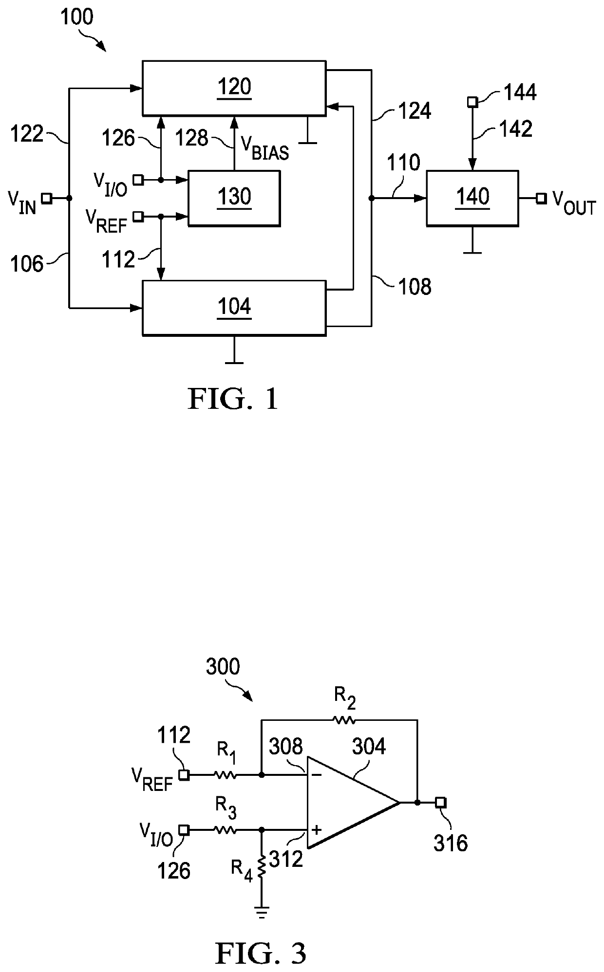
[0027]FIG. 1 is a high-level block diagram of a receiver 100 in accordance with an exemplary embodiment of the present disclosure. The receiver 100 is also referred herein as an input buffer. The receiver 100 is configured to operate in a wide range of input / output (I / O) voltage level (e.g., 1.8V-3.3V) and provide a low voltage output (e.g., 1.0 V).

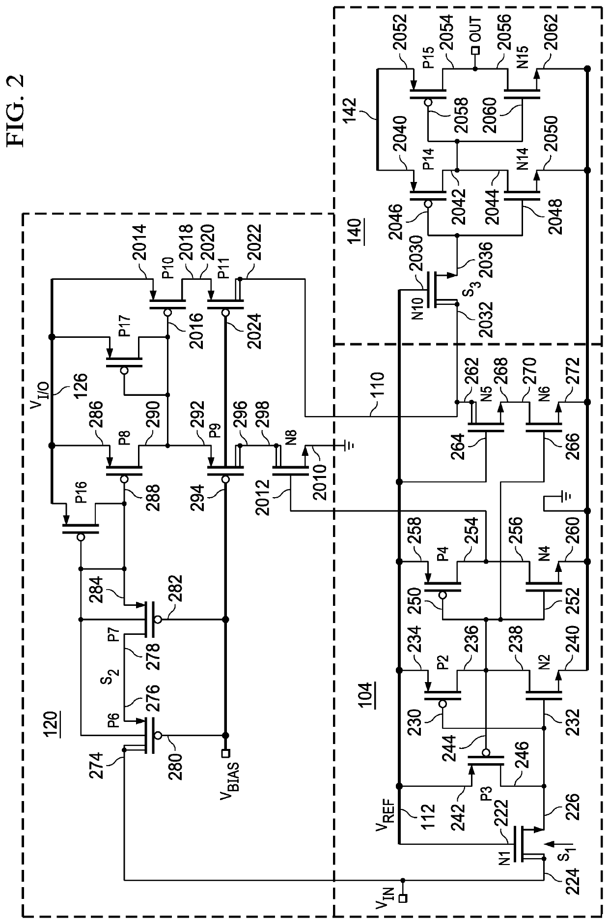
[0028]The receiver 100 includes a low-side buffer 104 having an input terminal 106 which can be coupled to an input signal Vin and having an output terminal 108 coupled to a buffer terminal 110 (also referred to as a buffer node 110). The low-side buffer 104 ...


PUM


Abstract

A receiver includes a low-side buffer having an input terminal coupled to receive an input signal and having an output terminal coupled to a buffer terminal. Responsive to the input signal being LOW, the low-side buffer is configured to couple the buffer terminal to ground. The receiver also includes a high-side buffer having an input terminal coupled to receive the input signal and having an output terminal coupled to the buffer terminal. Responsive to the input signal being HIGH, the high-side buffer is configured to provide an I / O voltage at the buffer terminal. The receiver also includes an output stage coupled to the buffer terminal and having a low voltage terminal configured to receive a low supply voltage. The output stage is configured to provide an output signal responsive to the I / O voltage at the buffer terminal, wherein the output signal is lower than the I / O voltage.

Description

CROSS REFERENCE TO RELATED APPLICATIONS[0001]This application claims priority from Indian provisional application No. 201941042292, filed Oct. 18, 2019, entitled “Wide Supply Voltage, Low Area, Low Power, High Speed Receiver Using Low-Voltage Gate Oxide”, assigned to the present assignee and incorporated herein by reference.BACKGROUND[0002]The disclosure generally relates to input buffers, and particularly to input buffers which operate in a wide range of I / O voltage level.DESCRIPTION OF THE RELATED ART[0003]Analog devices such as ethernet PHY and Universal Serial Bus (USB) generally require input buffers (also referred herein as receivers) to enable connection to a physical medium such as an optical fiber or a cable. Since input signals from a physical medium may have a range of voltage levels, the input buffers (or receivers) are configured to operate in a range of input / output (I / O) voltage levels (e.g., 1.8V-3.3V). However, the input buffers are often implemented with thin-oxide...

Claims


Application Information

Patent Timeline
Patent Type & Authority Patents(United States)
IPC IPC(8): H03K17/687H03K5/01H03K19/20H03K19/0175H03K19/0185H03K17/06
CPCH03K5/01H03K17/063H03K17/687H03K19/0175H03K19/0185H03K19/20H03K2217/0063H03K2217/0072
Inventor KALRA, PRANSHUSRINIVASAN, SRIKANTHRAJAGOPAL, DEVRAJ
Owner TEXAS INSTR INC
Why Eureka
Try Eureka