All-dielectric multi-band terahertz metamaterial absorber with randomly distributed units

A randomly distributed, all-dielectric technology, used in instruments, electrical components, optical components, etc., can solve the problem of periodically increasing the difficulty of product manufacturing, and achieve the effects of many absorption frequency points, high absorption rate, and various absorption modes.

Active Publication Date: 2021-07-23
XIAN UNIV OF TECH
View PDF11 Cites 0 Cited by
  • Summary
  • Abstract
  • Description
  • Claims
  • Application Information

AI Technical Summary

Problems solved by technology

[0004] However, strict periodicity increases the difficulty of product manufacturing, and also limits the generation of surface plasmon modes of different orders, and the cou

Method used


Image

  • All-dielectric multi-band terahertz metamaterial absorber with randomly distributed units
  • All-dielectric multi-band terahertz metamaterial absorber with randomly distributed units
  • All-dielectric multi-band terahertz metamaterial absorber with randomly distributed units

Examples


Example Embodiment

[0025] The present invention will be described in detail below with reference to the accompanying drawings and specific embodiments.

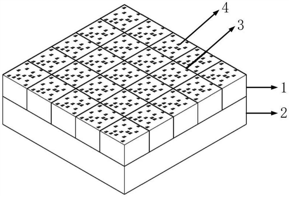
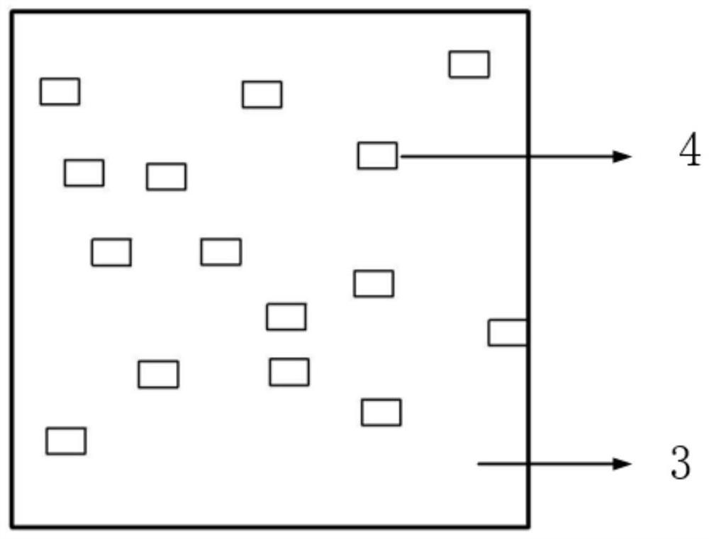
[0026] The full-scale multi-band genhera-ultrasound material absorber, including substrate layer 2 and structural layer 1, such as substrate layer 2 and structural layer 1, such as figure 1 As shown, the substrate layer 2 and the structural layer 1 are integrally doped silicon materials, and the structural layer 1 is uniformly divided on the structural layer 3, and several etch units 4 are provided in the mesh 3. The etching unit 4 is a square etchaven hole 5, a rectangular etch hole 6, a circular etching hole 7, a normal triangular etch hole 8, an irregular triangular etch hole 9, an elliptical etching hole 10. In any grid 3 does not overlap, a number of etch units 4 is provided without closely. Any grid 3 in the inner etch unit 4 is present at least one partial etch pattern is divided into adjacent mesh 3. The thickness of the substrate layer 2 i...


PUM

PropertyMeasurementUnit
Thicknessaaaaaaaaaa
Thicknessaaaaaaaaaa

Abstract

The invention discloses an all-dielectric multi-band terahertz metamaterial absorber with randomly distributed units, which comprises a substrate layer and a structural layer. The substrate layer and the structural layer are made of an integrated highly-doped silicon material, a plurality of grids are uniformly divided on the structural layer, and a plurality of etching units are arranged in the grids. The absorber has the characteristics that the stable absorption spectrum characteristic can be maintained under different unit arrangements, the absorption rate is high, the number of absorption frequency points is large, and the quality factor is high.

Description

technical field [0001] The invention belongs to the technical field of metamaterial absorbers, and relates to an all-dielectric multi-band terahertz metamaterial absorber with randomly distributed units. Background technique [0002] Terahertz metamaterials are artificial materials that work at terahertz frequencies and have extraordinary electromagnetic properties. According to the classification of material properties, they can generally be divided into metal metamaterials, all-dielectric metamaterials, and carbon-based metamaterials. Resonance occurs under the incidence of terahertz waves of frequency or frequency range, which has broad application prospects and application value in sensing, detection, imaging, communication and other application fields, attracting a lot of attention and triggering a research boom. [0003] In the current prior art, the metamaterial absorber is usually designed to have a periodic structure, and the overall structure of the absorber device...

Claims


Application Information

Patent Timeline
IPC IPC(8): H01Q17/00G02B1/00G02B5/00
CPCH01Q17/00G02B1/002G02B5/003
Inventor 王玥崔子健岳莉莎朱永强姚楠李存霞王馨梅
Owner XIAN UNIV OF TECH
Why Eureka
Try Eureka