
A Blind Insertion Structure of Vertical Interconnection between Boards and Its Realization Method
An implementation method and blind-mating technology, which are applied in the directions of printed circuits, printed circuits, and electrical components connected with non-printed electrical components, can solve the problem of high production costs, inability to use multiple connectors, and multi-layer blind-mating connections and structures. complex and other problems, to achieve the effect of reducing external stress and high reliability of vertical interconnection
- Summary
- Abstract
- Description
- Claims
- Application Information
AI Technical Summary
Problems solved by technology
Method used
Image

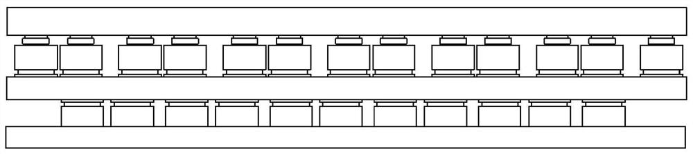
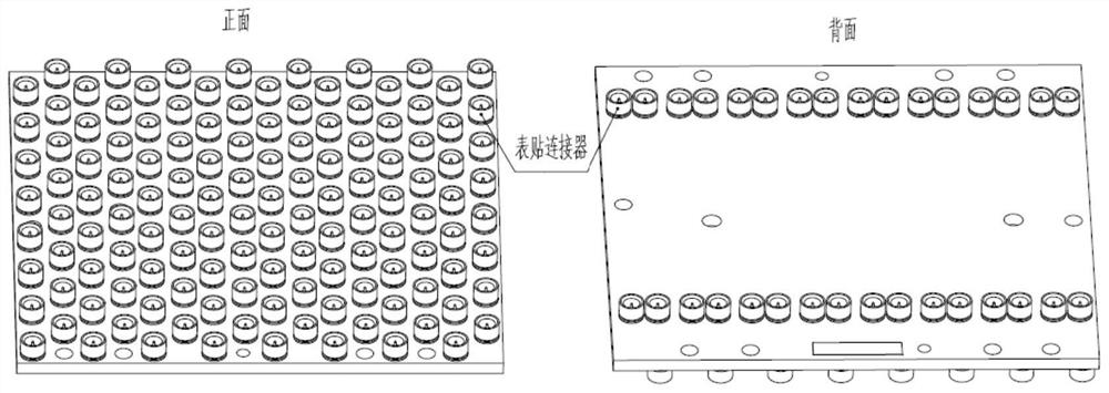
Examples
Embodiment
[0046] This embodiment provides a blind insertion structure for vertical interconnection between boards, such as Figure 9 As shown, the structure includes a mounting plate 1, a backing plate, a printed board assembly, a pressure plate, a mounting plate 2 and a spacer.
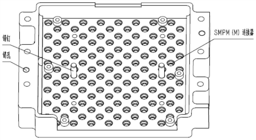
[0047] Among them, such as figure 2 As shown, there is a concave cavity on the mounting board 1, and the backing plate, the printed board assembly and the pressure plate are sequentially put into the concave cavity for positioning and assembly. The bottom of the cavity is equipped with an SMPM-M connector. There are two positioning pins at the bottom of the cavity. At the same time, pin holes are designed on the corresponding positions of the backing plate, printed board and pressure plate. The gap between the positioning pins and the pin holes is 0.02. -0.05mm, the chamfer of the pinhole opening is 0.3mm×45°; the left and right edges of the mounting plate 1 are also provided with positioning holes.
[0048...
PUM
 Abstract
Description
Claims
Application Information