Miniature electronic component welding device and a maintenance method thereof

A technology for electronic components and welding devices, which is applied in the direction of assembling printed circuits with electrical components, circuit devices, printed circuits connected with non-printed electrical components, etc., to achieve the effects of improving welding quality, avoiding short circuits, and improving electrical conductivity.

Active Publication Date: 2021-08-24
HUAINAN NORMAL UNIV
View PDF15 Cites 0 Cited by
  • Summary
  • Abstract
  • Description
  • Claims
  • Application Information

AI Technical Summary

Problems solved by technology

In addition, affected by the yield rate of microelectronic components, the microelectronic components soldered on the circuit board may be defective electronic components.

Method used


Image

  • Miniature electronic component welding device and a maintenance method thereof
  • Miniature electronic component welding device and a maintenance method thereof
  • Miniature electronic component welding device and a maintenance method thereof

Examples


Embodiment 1

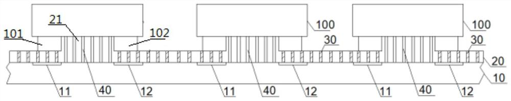
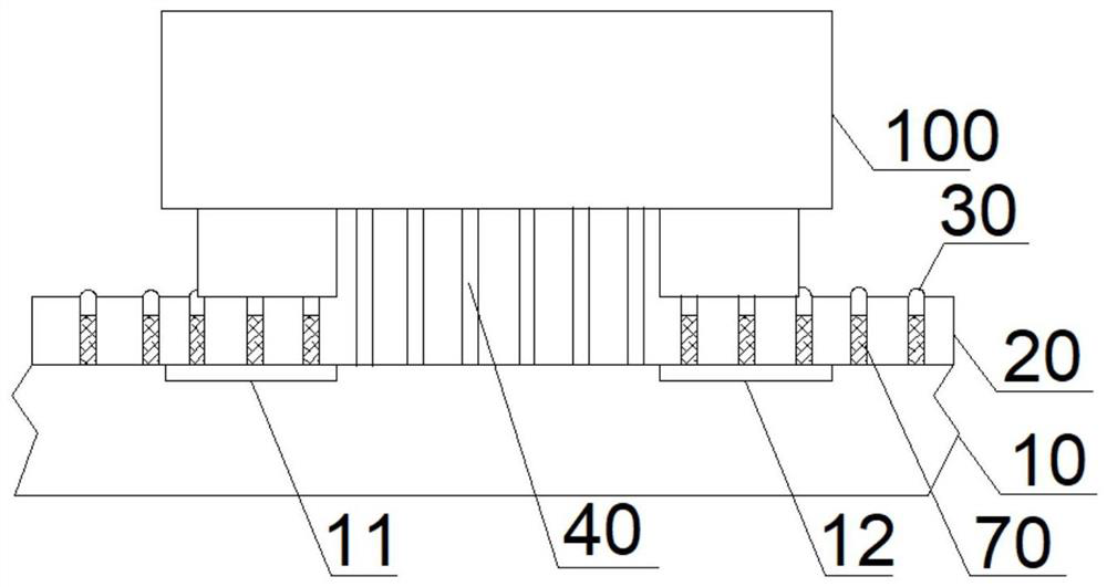
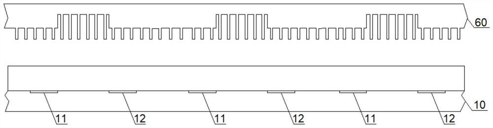
[0046] Such as figure 1 As shown, a kind of miniature electronic component soldering device of the present embodiment comprises a circuit backboard 10 and an intermediate communication structure; on the front surface of the circuit backboard 10, there are many groups of electrode contact pad groups arranged in an array; the intermediate communication structure is arranged on On the front surface of the circuit backboard 10 and cover the electrode contact pad group; the intermediate connection structure is used to movably set the microelectronic component 100, under the state that the microelectronic component 100 is movably arranged on the intermediate connection structure and applies a test signal to the circuit backplane 10 , the electrodes of the microelectronic component 100 are in corresponding contact with the electrode contact pads in the electrode contact pad group to conduct electricity.

[0047]It should be noted that the microelectronic components 100 here can be re...


PUM


Abstract

The invention discloses a miniature electronic component welding device and a maintenance method thereof. The miniature electronic component welding device comprises a circuit backboard and a middle communication structure; a plurality of electrode contact pad groups are arranged on the front surface of the circuit backboard in an array manner; the middle communication structure is arranged on the front surface and covers the electrode contact pad group; the middle communication structure is used for movably arranging the micro electronic element, and when the micro electronic element is arranged on the middle communication structure and a test signal is applied to the circuit backboard, the electrode of the micro electronic element is correspondingly contacted with the electrode contact pad in the electrode contact pad group for conduction. By determining whether contact conduction occurs or not, whether the miniature electronic element has a fault or not can be detected, if the miniature electronic element has the fault, the faulted miniature electronic element can be pulled out, a healthy miniature electronic element is replaced, whether the miniature electronic element is a defective pixel element or not can be detected under the condition that welding and fixing are not conducted, and timely replacement of the miniature electronic element is achieved; and meanwhile, the situation that the welding capacity is gradually lost due to the fact that the welding flux is repeatedly heated in a traditional overhauling method is avoided.

Description

technical field [0001] The invention relates to the field of semiconductor manufacturing, in particular to a miniature electronic component welding device and a maintenance method thereof. Background technique [0002] With the advancement of semiconductor and integrated circuit technology, the size of electronic components such as diodes, transistors, sensors, and actuators is getting smaller and smaller, even reaching the level of less than 100 microns. When using these microelectronic components to manufacture electronic equipment, it is necessary to solder these microelectronic components to corresponding positions on the circuit board one by one. In addition, affected by the yield rate of the microelectronic components, the microelectronic components soldered on the circuit board may be defective electronic components. [0003] After detecting a dead point microelectronic component, it is generally necessary to heat the solder of the dead point electronic component to ...

Claims


Application Information

Patent Timeline
Patent Type & Authority Applications(China)
IPC IPC(8): H05K1/18H05K1/02H05K3/22H05K3/34
CPCH05K1/18H05K1/0213H05K3/34H05K3/225
Inventor 葛先雷许静雯王杨刘音轩雪飞杨帅斌葛竹红李本杰
Owner HUAINAN NORMAL UNIV
Why Eureka
Try Eureka