Stamping type stepped bonding pad PCB and manufacturing technology

A manufacturing technology, stamping technology, applied in the direction of printed circuit manufacturing, the formation of electrical connection of printed components, and the electrical connection of printed components, etc., can solve problems such as difficult to solve problems, project schedule, cost impact, etc., and achieve the effect of making up for insufficient height

Pending Publication Date: 2021-08-27
ZHUHAI YUANSHENG ELECTRONICS SCI & TECH
View PDF0 Cites 0 Cited by
  • Summary
  • Abstract
  • Description
  • Claims
  • Application Information

AI Technical Summary

Problems solved by technology

But no matter which method may affect the progress and cost of the project, it may even be difficult to solve the problem

Method used


Image

  • Stamping type stepped bonding pad PCB and manufacturing technology
  • Stamping type stepped bonding pad PCB and manufacturing technology
  • Stamping type stepped bonding pad PCB and manufacturing technology

Examples


Embodiment Construction

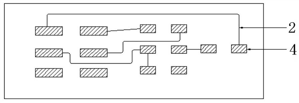
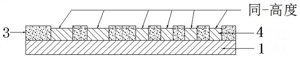
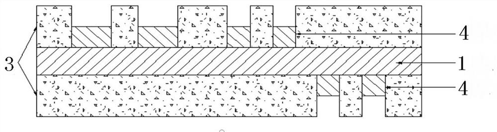
[0023] Such as image 3 with Figure 4 said, image 3 It is a simple schematic diagram of a double-sided semi-finished product, in which only the substrate, pads and cover film are shown. The double-sided board can be made according to the conventional method. In order to increase the operability, the finished PCB die-cuts the shape and cannot be cut into single pieces. In this embodiment, the present invention includes a PCB substrate 1, which is arranged on the PCB The circuit 2 on the circuit 1 and the solder resist ink or cover film 3 covering the circuit 2, the stamped stepped pad PCB also includes a circuit that is electrically connected to the circuit 2 and is not covered by the solder resist ink or the A plurality of pads 4 covered by the cover film 3, at least one of the pads 4 is a stamped stepped pad, and a stamped boss 5 is arranged on the top of the stamped stepped pad, and the bottom of the stamped stepped pad A concave cavity 6 corresponding to the stamping b...


PUM


Abstract

The invention discloses and provides a stamping type stepped bonding pad PCB and a manufacturing technology. a part of PCB bonding pads have stepped height difference and are not on the same plane; and after the PCB is applied, conventional components can be adopted to realize a product design function, so that high redevelopment cost and time cost of the components are avoided. The stamping type stepped bonding pad PCB comprises a PCB base material, a circuit arranged on the PCB base material and solder resist ink or a covering film covering the circuit. The stamping type stepped bonding pad PCB further comprises a plurality of bonding pads which are electrically connected with the circuit and are not covered by the solder resist ink or the covering film; at least one bonding pad is a stamping type step bonding pad; a stamping boss is arranged on the upper surface of the stamping type stepped bonding pad; a concave cavity corresponding to the stamping boss is arranged in the lower surface of the stamping type stepped bonding pad; and a base material protrusion filled in the concave cavity is arranged on the PCB base material. The manufacturing technology is mainly characterized in that a boss is stamped on a bonding pad which needs to be heightened through die stamping on the PCB which is provided with the covering film and is not subjected to surface electroplating. The invention is applied to the technical field of PCB manufacturing.

Description

technical field [0001] The invention relates to a PCB and its manufacturing technology, in particular to a stamped stepped pad PCB and its manufacturing technology. Background technique [0002] With the development of electronic technology, the PCBs used in electronic equipment are becoming more and more complex. In order to realize complex functions, PCBs generally need to be equipped with components. In some occasions, in addition to the beautiful appearance of the board, it is more important to realize the product design function, which requires special requirements for the installation accuracy of some components. For example, some require that one or more components need to ensure the same height, such as some sensors or something. [0003] The production of components usually has a fixed height, thickness and other dimensions according to certain standards. Since the PCB pads are all planar, they are at the same height. figure 1 , figure 2 . In this way, some com...

Claims


Application Information

Patent Timeline
Patent Type & Authority Applications(China)
IPC IPC(8): H05K1/11H05K3/40
CPCH05K1/11H05K3/4007
Inventor 杨婵林均秀邵家坤
Owner ZHUHAI YUANSHENG ELECTRONICS SCI & TECH
Why Eureka
Try Eureka