Method for manufacturing device for chip testing

A manufacturing method and chip testing technology, which can be used in measuring devices, electronic circuit testing, and components of electrical measuring instruments, etc., and can solve problems such as poor contact, inaccurate chip test results, and easily skewed probes.

Active Publication Date: 2021-09-10
SUZHOU TF AMD SEMICON CO LTD
View PDF14 Cites 0 Cited by
  • Summary
  • Abstract
  • Description
  • Claims
  • Application Information

AI Technical Summary

Problems solved by technology

[0004] During the above test process, the probes of the test base are e

Method used


Image

  • Method for manufacturing device for chip testing
  • Method for manufacturing device for chip testing
  • Method for manufacturing device for chip testing

Examples


Embodiment Construction

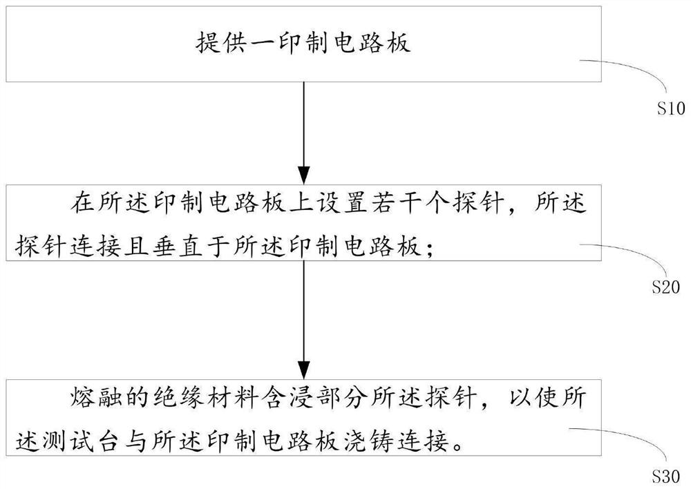
[0031] The application will be further described in detail below in conjunction with the accompanying drawings and embodiments. It should be understood that the specific embodiments described here are only used to explain related inventions, rather than to limit the invention. It should also be noted that, for ease of description, only parts related to the invention are shown in the drawings.

[0032] It should be noted that, in the case of no conflict, the embodiments in the present application and the features in the embodiments can be combined with each other. The present application will be described in detail below with reference to the accompanying drawings and embodiments.

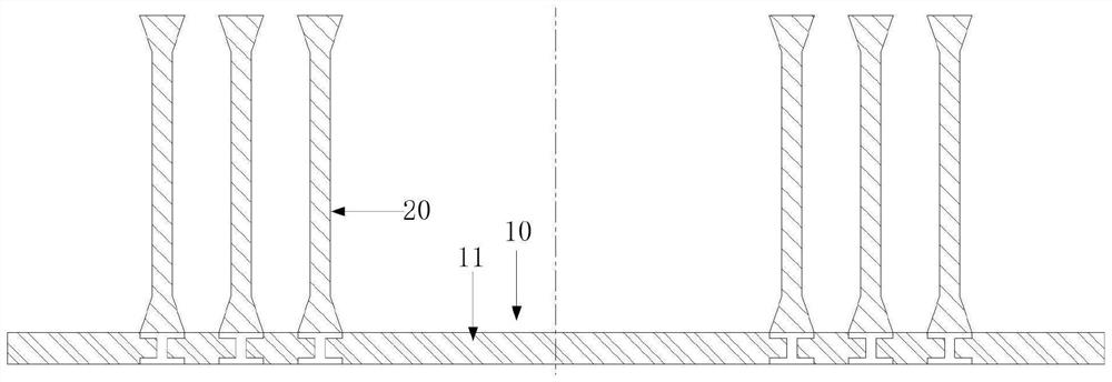
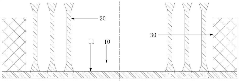
[0033] Figure 8 A schematic structural diagram of the first device for chip testing is shown.

[0034] The first device for chip testing includes: a test base 10 , a test platform 40 , probes 20 and an insulating sleeve 60 . The test base 10 includes a printed circuit board 11 disposed on the s...


PUM


Abstract

The invention relates to the technical field of chips, and discloses a method for manufacturing a device for chip testing. The method comprises the steps that a printed circuit board is provided; a plurality of probes are arranged on the printed circuit board, and the probes are connected with and perpendicular to the printed circuit board; parts of the probes are impregnated by a molten insulating material, so that a test bench is in casting connection with the printed circuit board. According to the invention, a test base is in casting connection with the test bench, so that the probes of the test base and the test bench are always relatively static, thereby avoiding the inclination or bending of the probes caused by the frequent penetration or penetration of the probes out of the through holes of the test bench, and facilitating the stable electric connection of a to-be-tested chip and the test base.

Description

technical field [0001] The present invention generally relates to the field of chip technology, and in particular to a device manufacturing method for chip testing. Background technique [0002] A chip generally refers to the carrier of an integrated circuit, and is also the result of the design, manufacture, packaging, and testing of an integrated circuit. It is usually an independent whole that can be used immediately. After the chip is manufactured, strict tests are required, such as aging test and optical power test. [0003] In the related art, the chip testing device includes a chip carrier and a test base. During the test, the chip to be tested is placed on the chip carrier, and the probes of the test base need to pass through the holes of the chip carrier and the chip to be tested. Electrically connected to achieve chip testing. [0004] During the above test process, the probes of the test base are easily skewed, resulting in poor contact and inaccurate chip test ...

Claims


Application Information

Patent Timeline
IPC IPC(8): G01R31/28G01R1/073
CPCG01R31/2886G01R31/2898G01R1/07364
Inventor 刘在福曾昭孔郭瑞亮陈武伟
Owner SUZHOU TF AMD SEMICON CO LTD
Why Eureka
Try Eureka