
Method and device for calibrating OM and SEM coordinate relation, equipment and storage medium

A coordinate relationship and marking point technology, applied in the field of calibrating OM and SEM coordinate relationship, can solve problems such as deviation, time-consuming and labor-intensive

Active Publication Date: 2021-09-10
ZHONGKE JINGYUAN ELECTRON LTD
View PDF9 Cites 0 Cited by
  • Summary
  • Abstract
  • Description
  • Claims
  • Application Information

AI Technical Summary

Problems solved by technology

In general, the calibration of the coordinate relationship between OM and SEM of EBI equipment is mainly done manually. This method is not only time-consuming and labor-intensive, but also prone to deviations caused by human factors.

Method used


Image

  • Method and device for calibrating OM and SEM coordinate relation, equipment and storage medium
  • Method and device for calibrating OM and SEM coordinate relation, equipment and storage medium
  • Method and device for calibrating OM and SEM coordinate relation, equipment and storage medium

Examples


Embodiment Construction

[0054] Various exemplary embodiments, features, and aspects of the present disclosure will be described in detail below with reference to the accompanying drawings. The same reference numbers in the figures indicate functionally identical or similar elements. While various aspects of the embodiments are shown in drawings, the drawings are not necessarily drawn to scale unless specifically indicated.

[0055] The word "exemplary" is used exclusively herein to mean "serving as an example, embodiment, or illustration." Any embodiment described herein as "exemplary" is not necessarily to be construed as superior or better than other embodiments.

[0056] In addition, the terms "first" and "second" are used for descriptive purposes only, and cannot be interpreted as indicating or implying relative importance or implicitly specifying the quantity of indicated technical features. Thus, a feature defined as "first" and "second" may explicitly or implicitly include one or more of these...


PUM


Abstract

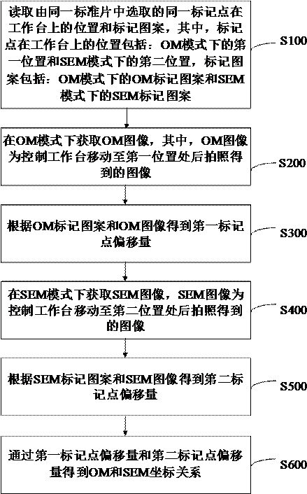
The invention discloses a method for calibrating an OM and SEM coordinate relation. The method comprises the steps: reading a position and a mark pattern of the same mark point selected from the same standard film on a workbench, obtaining an OM image in an OM mode, obtaining a first mark point offset according to the OM mark pattern and the OM image, obtaining an SEM image in an SEM mode, the SEM image being an image obtained by photographing after the workbench is controlled to move to a second position, obtaining a second mark point offset according to an SEM mark pattern and the SEM image, and obtaining an OM and SEM coordinate relation through the first mark point offset and the second mark point offset. In this way, the calibration process before electron beam detection and feature size measurement in a semiconductor manufacturing process is automatically processed, and the method not only eliminates the influence of human factors and environmental factors (temperature and the like), but also improves the detection efficiency.

Description

technical field [0001] The present disclosure relates to the technical field of semiconductor manufacturing and detection, and in particular to a method, device, device and storage medium for calibrating the coordinate relationship between OM and SEM. Background technique [0002] In recent years, with the development of new technologies such as the Internet of Things and artificial intelligence, the demand for semiconductor chips is increasing day by day, and the chip manufacturing process is becoming more and more refined. The increasingly refined production process will reduce the chip power and also limit the production yield of semiconductor manufacturing. In the semiconductor manufacturing process of the technology node below 28nm, the production yield can be effectively improved by means of electron beam defect inspection (EBI). Before electron beam defect detection, it is essential for the calibration of EBI equipment, this step will directly affect the defect detec...

Claims


Application Information

Patent Timeline
IPC IPC(8): G06T7/00G06T7/62G06T7/73G06K9/62
CPCG06T7/001G06T7/62G06T7/73G06T2207/10004G06T2207/30148G06F18/22
Inventor 甘远薛磊韩春营俞宗强蒋俊海
Owner ZHONGKE JINGYUAN ELECTRON LTD
Learn More