

Semiconductor device and manufacturing method thereof
A semiconductor and device technology, applied in the field of semiconductor devices and their preparation, can solve the problems affecting the output quantity of single-wafer devices and the effective area occupation of devices, so as to improve the moisture resistance, reduce the area, and reduce the occupation of the area Effect
- Summary
- Abstract
- Description
- Claims
- Application Information
AI Technical Summary
Problems solved by technology
Method used
Image

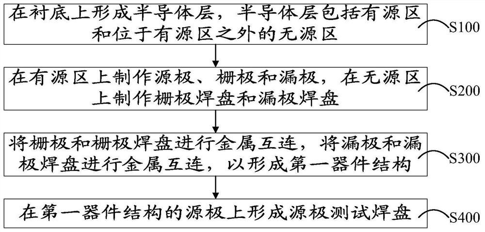
Examples
Embodiment Construction
[0050] The terminology used herein is for the purpose of describing particular embodiments only and is not intended to limit the present disclosure.
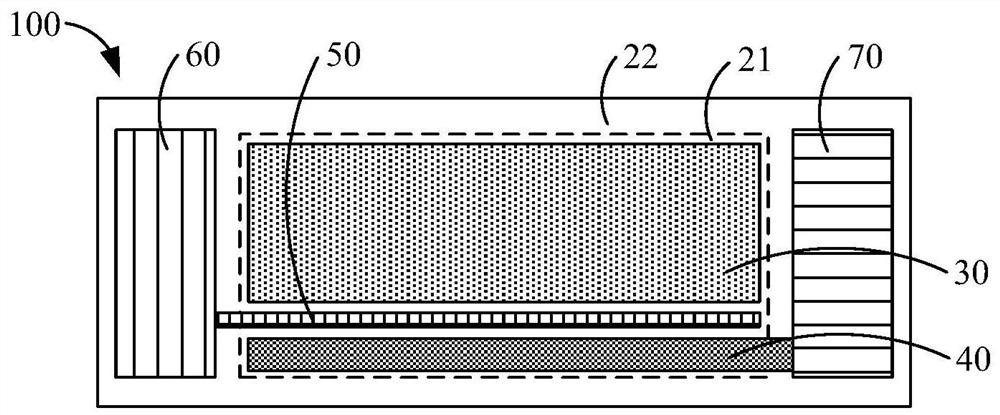
[0054] S100, forming a semiconductor layer 20 on the substrate 10, the semiconductor layer 20 comprising an active region 21 and a space between the active region 21
[0056] S300, the gate 50 and the gate pad 60 are metal interconnected, and the drain 40 and the drain pad 70 are metal interconnected
[0058] It should be noted that the gate pad 60 and the drain pad 70 of the present application are arranged in the inactive region 22, wherein the gate pad
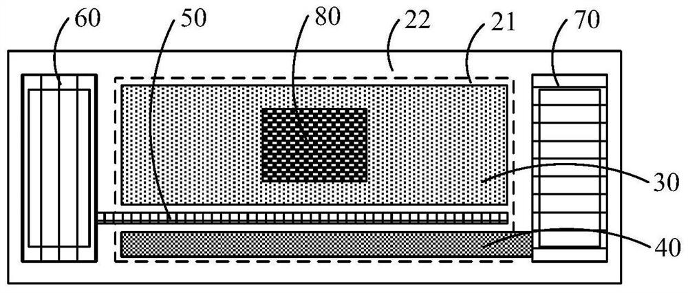
[0059] S400, a source test pad 80 is formed on the source electrode 30 of the first device structure 100, as shown in FIG. 3 .
[0060] That is, in the present embodiment, the source test pad 80 is provided on the source electrode 30 of the active region 21. So, the electrical test
[0062] Please refer to FIG. 8 , optionally, in the above step S400, a source test is formed on th...
PUM
| Property | Measurement | Unit |
|---|---|---|
| thickness | aaaaa | aaaaa |
Abstract
Description
Claims
Application Information