A test method for through-silicon via adapter board

A test method and adapter board technology, applied in the direction of the measuring device shell, etc., can solve problems such as damage, affecting packaging quality, holding and testing difficulties, etc.

Active Publication Date: 2016-09-21
NAT CENT FOR ADVANCED PACKAGING CO LTD
View PDF7 Cites 0 Cited by
  • Summary
  • Abstract
  • Description
  • Claims
  • Application Information

AI Technical Summary

Problems solved by technology

Because the TSV interposer is very thin, the material is brittle, and the density of pads (bumps) is high, double-sided testing is required, and traditional testing techniques are difficult to use
As the I / O density on the semiconductor chip is getting higher and higher, and the size of the pad is getting smaller and smaller, when performing electrical tests on the TSV adapter board, see figure 1 , the existing electrical test adopts the method of probe contact, the probe 3 is contacted with the pad 2 on the TSV adapter board 1, the TSV adapter board to be tested is drawn out, and the silicon through the probe is realized. Electrical testing of through-hole adapter boards. This test method will cause scratches and damage to through-silicon via adapter boards, which will affect the quality of subsequent packaging. The thickness of silicon wafers is getting thinner and thinner, which makes it difficult to hold and test. It affects the electrical test efficiency and test effect of the TSV adapter board

Method used


Image

  • A test method for through-silicon via adapter board
  • A test method for through-silicon via adapter board
  • A test method for through-silicon via adapter board

Examples


Embodiment Construction

[0012] The invention will be described in detail below in conjunction with the accompanying drawings, but this embodiment is not limited to the invention. The structural, method or functional changes made by those skilled in the art based on this embodiment are all included in the present invention. Within the scope of protection.

[0013] A test method for a through silicon via transfer board includes the following steps:

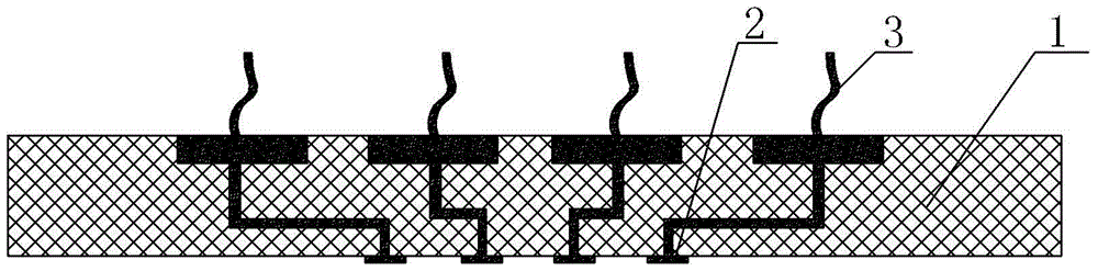
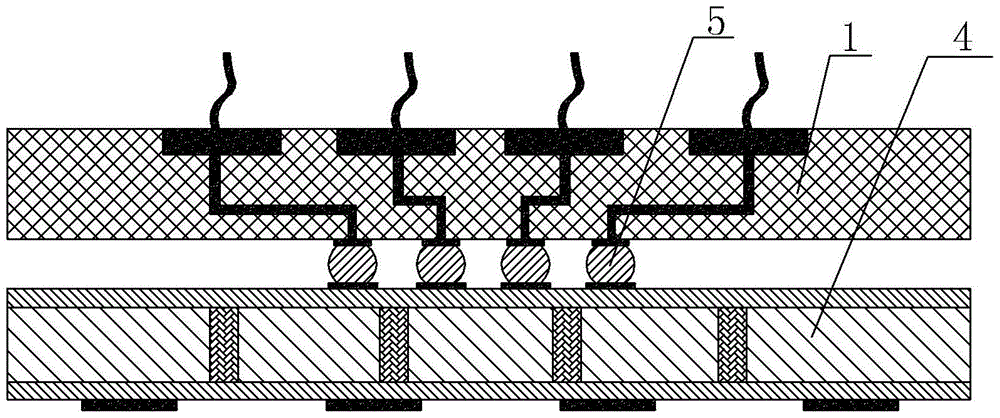
[0014] see figure 2 , (1). Preparation of the test adapter board. Prepare a pressure solder joint (pad) 2 on the test adapter board 1, and use the probe lead 3 to lead the pad out of the other side of the test adapter board 1; see image 3 (2). Use temporary welding to physically connect the bumps 5 (solder balls) on the TSV adapter board 4 to the test adapter board 1;

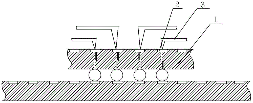
[0015] see Figure 4 , (3). Set the test adapter board 1 on both sides of the TSV adapter board 4 correspondingly, and use the probe leads 3 on the test adapter board 1 to connect the pads on t...


PUM


Abstract

The invention provides a through-silicon via patch board testing method. By means of the method, electric testing can be conducted on a through-silicon via patch board simply and conveniently, the through-silicon via patch board is effectively prevented from being scratched and damaged during testing, the electric testing efficiency of the through-silicon via patch board and the testing effect of the through-silicon via patch board are guaranteed, and the packaging quality of a follow-up chip is guaranteed. The through-silicon via patch board testing method is characterized by comprising the following steps that (1) patch board equipment is tested, pads are manufactured on a testing patch board, and probe leads are used for leading a welding disk out of the other face of the testing patch board; (2) a temporary welding method is used for physically connecting protrusions (solder balls) on the through-silicon via patch board to the testing patch board.

Description

Technical field [0001] The invention relates to the technical field of microelectronic testing in the microelectronics industry, in particular to a testing method for a through silicon via transfer board. Background technique [0002] With the development of large-scale integrated circuits, the lines are getting thinner and thinner, and the traditional two-dimensional semiconductor manufacturing technology is facing huge challenges. The use of three-dimensional integration technology can shorten the interconnection path, reduce the delay, reduce the power consumption, and obtain higher performance. Become the development trend of the semiconductor industry in the future. Through silicon via technology is the core technology to achieve three-dimensional integration. It forms vertical interconnection channels by directly making conductive vias on different types of chips. At present, one method is to fabricate an interposer through silicon vias, and realize high-density interconne...

Claims


Application Information

Patent Timeline
Patent Type & Authority Patents(China)
IPC IPC(8): G01R1/04
Inventor 靖向萌
Owner NAT CENT FOR ADVANCED PACKAGING CO LTD
Why Eureka
Try Eureka