Elastic wave device package and module including elastic wave device
A device packaging and elastic wave technology, applied in electrical components, impedance networks, etc., can solve the problem that elastic wave devices do not have a structure, and achieve the effect of suppressing ESD damage and improving ESD tolerance
- Summary
- Abstract
- Description
- Claims
- Application Information
AI Technical Summary
Problems solved by technology
Method used
Image

Examples
no. 1 example
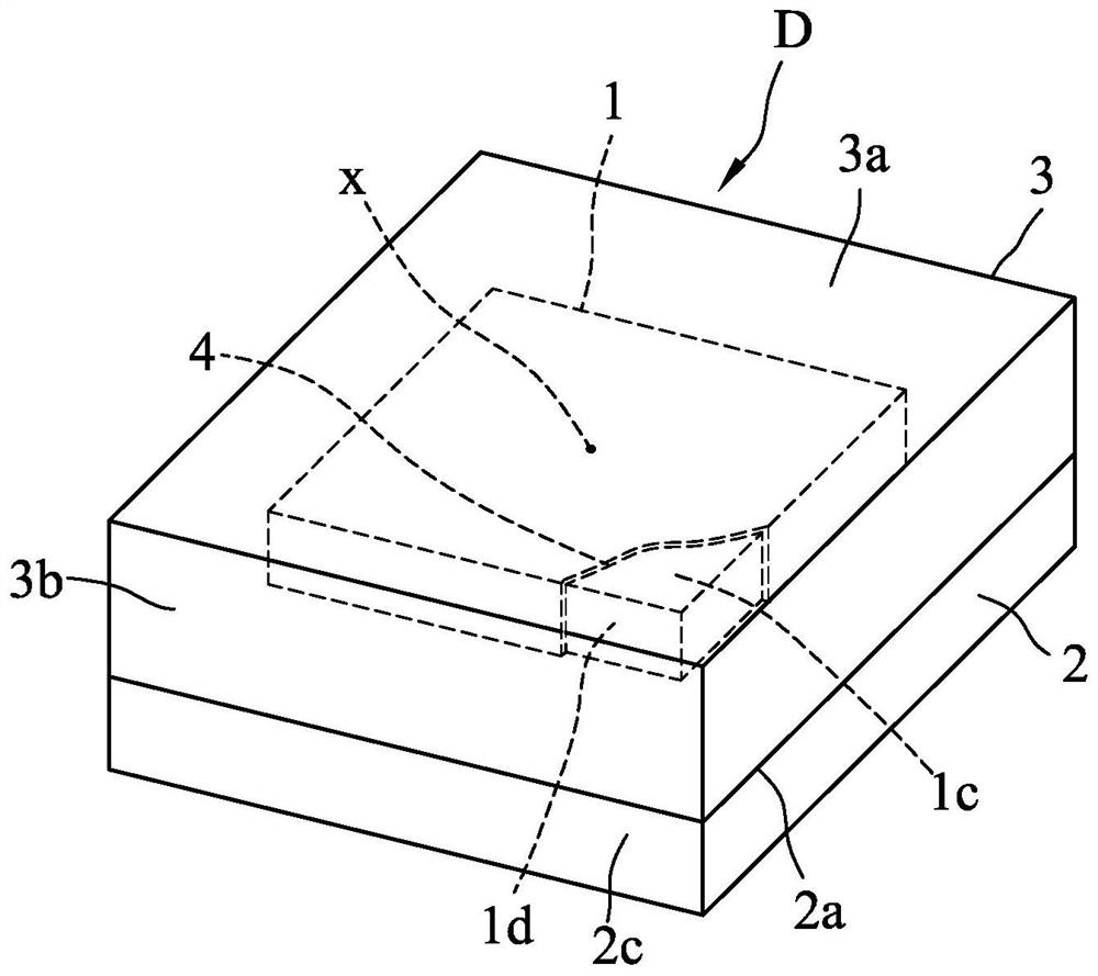
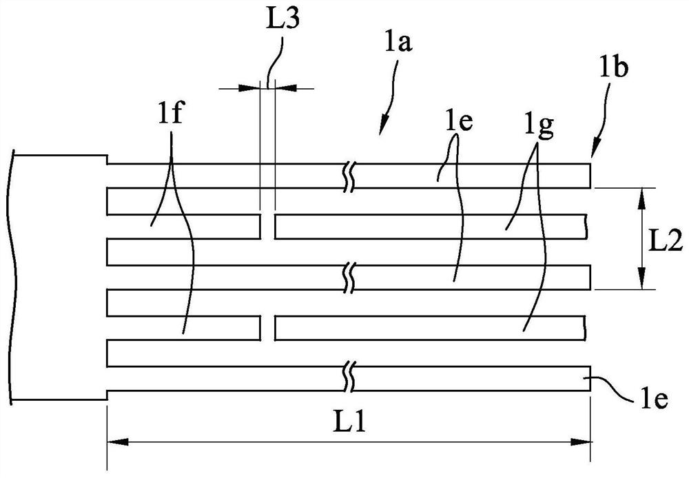
[0047] figure 1 and figure 2 Referring to the first embodiment of the present invention, the conductive resin layer 4 covers the entire area of the facing surface 1 c of the elastic wave device 1 and the end surface 1 d of the elastic wave device 1 .
[0048] Thereby, for example, when the elastic wave device package D is placed in a high electric field (in an atmosphere where static electricity is generated), when the elastic wave device package D generates charges due to friction between each other, or when cutting (Dicing ) process to remove the elastic wave device package D from the dicing tape (Dicing Tape), etc., can prevent the comb-shaped electrodes 1b constituting the elastic wave device 1 from being concentratedly charged.
[0049] In addition, the elastic wave device package D can be configured in a state where the conductive resin layer 4 and the encapsulating resin 3 are highly adhered to each other and are integrally molded firmly. The thickness of the condu...
no. 2 example
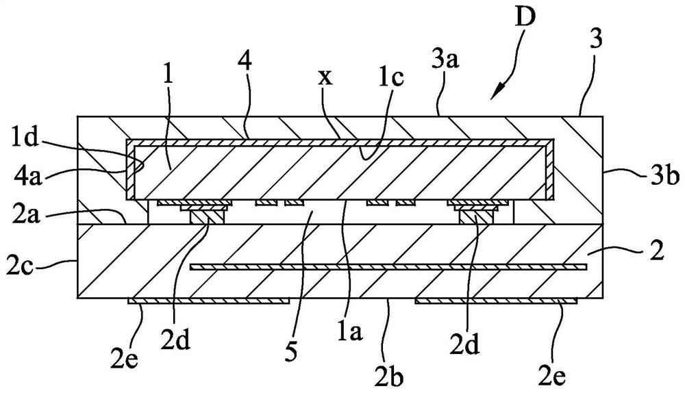
[0051] Figure 4 Referring to the second embodiment of the present invention, the conductive resin layer 4 includes a portion 4a connected to and covering the end face 1d of the elastic wave device 1, and a portion extending and covering at least part of the mounting side of the package substrate 2. Prolongation 4b of surface 2a.
[0052] Such as Figure 4 As shown in , the extension part 4b has a first part 4c that hangs down from the part 4a of the end surface 1d and contacts the surface 2a, and extends outward from the lower end of the first part 4c and terminates at the opposite package substrate. The end face 2c of 2 is the second portion 4d located slightly inside. and, if Figure 4 As shown, the conductive resin layer 4 has the first portion 4c and the second portion 4d no matter it is disposed at any position around the center x of the elastic wave device 1 .
[0053] In this case, firstly, the area of the conductive resin layer 4 can be increased, thereby making...
no. 3 example
[0056] Figure 5 Referring to the third embodiment of the present invention, the extension portion 4b is electrically connected to the electrode 2f formed on the mounting side surface 2a of the package substrate 2 and connected to the external connection terminal 2e.
[0057] In such a case, since the charges in the conductive resin layer 4 can be easily discharged through the external connection terminal 2e, the ESD resistance of the elastic wave device package D can be improved. At this time, if the conductive resin layer 4 with an appropriate impedance value is used together, the discharge can be performed slowly, so that the high peak value of the electric field can be suppressed and the ESD tolerance can be improved.
PUM
| Property | Measurement | Unit |
|---|---|---|
| Thickness | aaaaa | aaaaa |
Abstract
Description
Claims
Application Information
 - R&D
- Intellectual Property
- Life Sciences
- Materials
- Tech Scout
- Unparalleled Data Quality
- Higher Quality Content
- 60% Fewer Hallucinations
Browse by: Latest US Patents, China's latest patents, Technical Efficacy Thesaurus, Application Domain, Technology Topic, Popular Technical Reports.
© 2025 PatSnap. All rights reserved.Legal|Privacy policy|Modern Slavery Act Transparency Statement|Sitemap|About US| Contact US: help@patsnap.com