A bonded package and its preparation method
A package and bonding technology, which is applied in semiconductor/solid-state device manufacturing, semiconductor devices, electric solid-state devices, etc., can solve the problems of bonded body function failure, bonded body easy to peel and collapse, etc.
- Summary
- Abstract
- Description
- Claims
- Application Information
AI Technical Summary
Problems solved by technology
Method used
Image

Examples
Embodiment Construction
[0035] In order to better understand the technical solutions of the present invention, the embodiments of the present invention will be described in detail below in conjunction with the accompanying drawings. Based on the embodiments of the present invention, all other embodiments obtained by persons of ordinary skill in the art without creative efforts fall within the protection scope of the present invention.
[0036] The present invention proposes a method for preparing a bonded package, comprising the following steps:
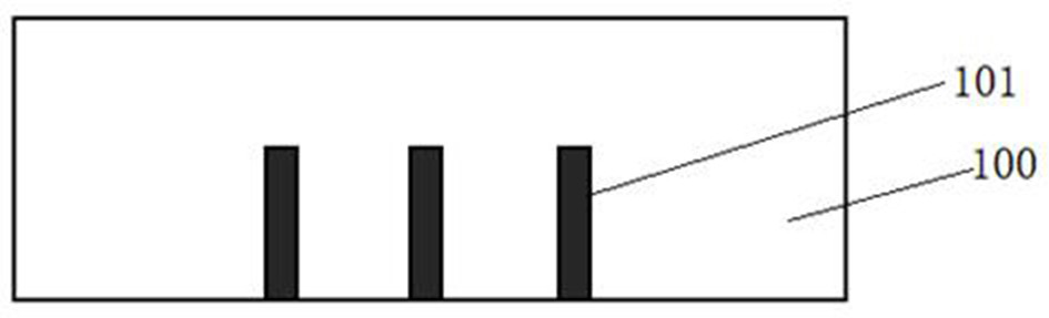
[0037] Step (1): providing a first semiconductor die having through-silicon vias therein.
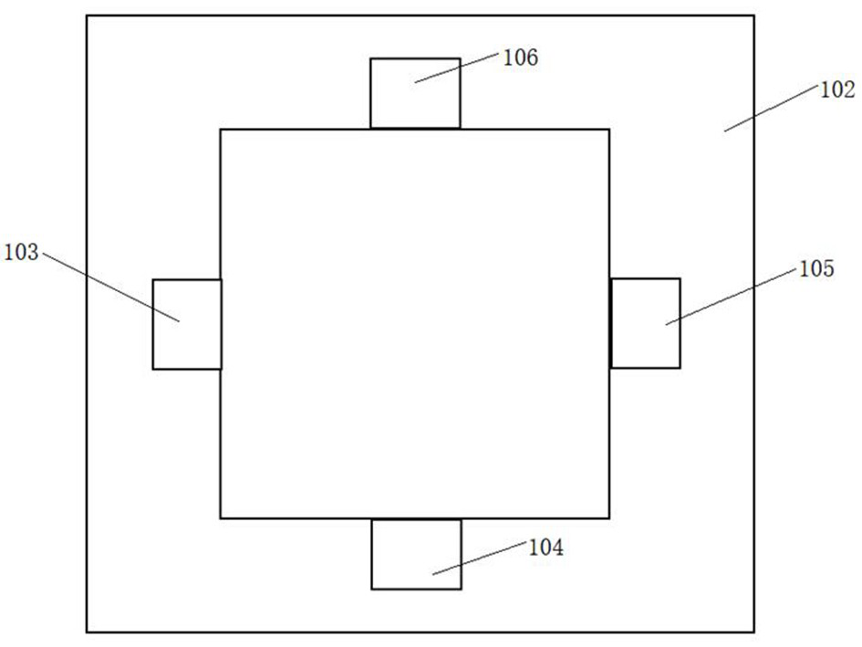
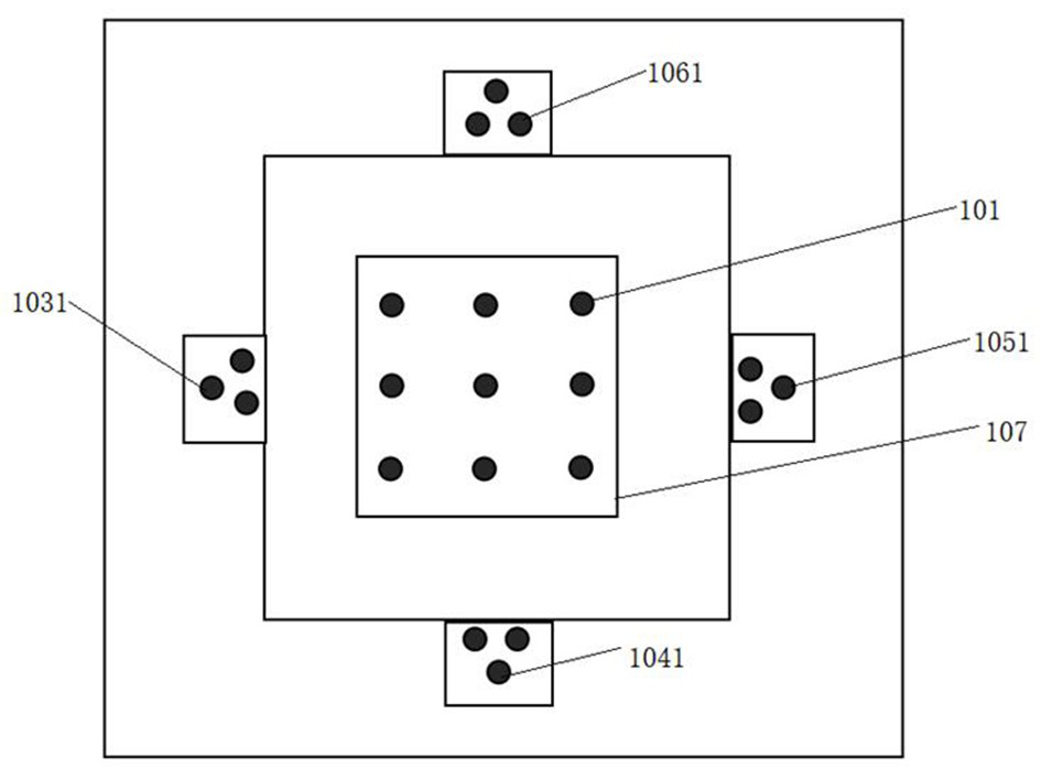
[0038] Step (2): disposing the first semiconductor die on the first substrate, and then performing etching on the first semiconductor die to respectively form first, second, third, and fourth bonding portions, the first, second, third, and fourth bonding portions respectively protrude from the first, second, third, and fourth bonding portions of the first semiconduc...
PUM
 Abstract
Description
Claims
Application Information