High-speed large-area-array infrared imaging circuit

A technology of infrared imaging and large area array, applied in the direction of electric radiation detector, radiation pyrometry, measuring device, etc., to reduce acquisition noise, reduce target loss, and improve the effect of sensitive area

Pending Publication Date: 2021-11-05
SHANGHAI AEROSPACE CONTROL TECH INST
View PDF4 Cites 0 Cited by
  • Summary
  • Abstract
  • Description
  • Claims
  • Application Information

AI Technical Summary

Problems solved by technology

The design of the detector acquisition circuit with high frame rate and large area array has yet to be verified

Method used


Image

  • High-speed large-area-array infrared imaging circuit
  • High-speed large-area-array infrared imaging circuit
  • High-speed large-area-array infrared imaging circuit

Examples


Embodiment Construction

[0047] Exemplary embodiments of the present disclosure will be described in more detail below with reference to the accompanying drawings. Although exemplary embodiments of the present disclosure are shown in the drawings, it should be understood that the present disclosure may be embodied in various forms and should not be limited by the embodiments set forth herein. Rather, these embodiments are provided for more thorough understanding of the present disclosure and to fully convey the scope of the present disclosure to those skilled in the art. It should be noted that, in the case of no conflict, the embodiments of the present invention and the features in the embodiments can be combined with each other. The present invention will be described in detail below with reference to the accompanying drawings and examples.

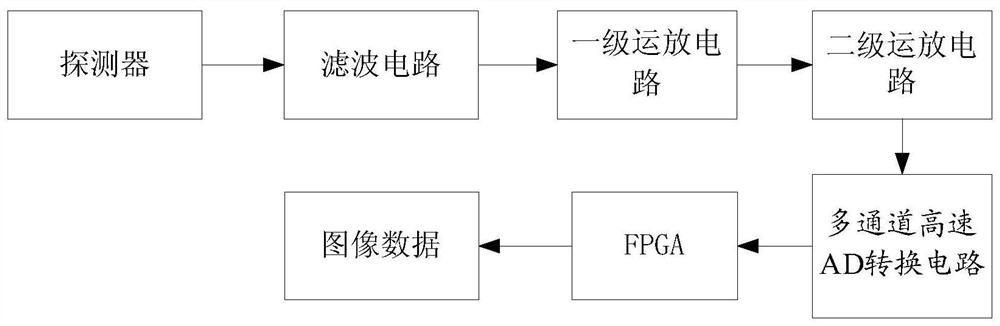
[0048] figure 1 It is a structural block diagram of the high-speed large area array infrared imaging circuit of the present invention. like figure 1 As sho...


PUM


Abstract

The invention discloses a high-speed large-area-array infrared imaging circuit. The circuit comprises a filter circuit, a first-stage operational amplifier circuit, a second-stage operational amplifier circuit, a multi-channel high-speed AD conversion circuit and a processor FPGA; the processor FPGA completes configuration of the detector and the multi-channel high-speed AD conversion circuit, so that the detector normally outputs an image signal, and the multi-channel high-speed AD conversion circuit can start to collect the signal; the filter circuit carries out low-pass filtering on the original image signal and then sends the original image signal to the first-stage operational amplifier circuit; the first-stage operational amplifier circuit follows and biases the filtered signal; the second-stage operational amplifier circuit carries out scaling and differential transformation on the signal processed by the first-stage operational amplifier; the multi-channel high-speed AD conversion circuit acquires a differential signal and digitalizes the differential signal and sends the differential signal to the processor FPGA; and the processor FPGA acquires data of the multi-channel high-speed AD conversion circuit, packages the data and sends the data to a next-level system. The image acquisition noise is reduced, the image acquisition speed is improved, and the sensitivity range of a product is improved.

Description

technical field [0001] The invention belongs to the technical field of microelectronics and optoelectronics, and in particular relates to a high-speed large-area array infrared imaging circuit. Background technique [0002] Infrared imaging technology has become a research hotspot in the world today in the military field. The advent of the third generation of infrared detectors has brought infrared imaging technology to another level in military applications. High frame rate and large area array detectors also emerged as the times require. The application of high frame rate and large area array infrared detector in the seeker system greatly improves the performance of the seeker. Multi-arrays can increase the sensitivity threshold of the product, allowing the product to detect farther targets; high frame rates can quickly update the target information of the product, making the pre-push trajectory of the missile more accurate, increasing the bandwidth, reducing target loss...

Claims


Application Information

Patent Timeline
Patent Type & Authority Applications(China)
IPC IPC(8): G01J5/10G01J5/00
CPCG01J5/10G01J5/00
Inventor 苗壮李宁珍龚瑞关智聪刘菁菁龚文张丰收许羽
Owner SHANGHAI AEROSPACE CONTROL TECH INST
Why Eureka
Try Eureka