Selective testing device for semiconductor material research and development

A technology for selecting test and device materials, which is applied in the direction of measuring devices, measuring device casings, and parts of electrical measuring instruments. It can solve problems such as single structure, inability to fix bolts elastically prevent loosening, and inconvenient disassembly and assembly.

Active Publication Date: 2021-11-05
南通优睿半导体有限公司
View PDF5 Cites 0 Cited by
  • Summary
  • Abstract
  • Description
  • Claims
  • Application Information

AI Technical Summary

Problems solved by technology

[0007] In order to solve the above-mentioned technical problems, the present invention provides a selective testing device for the research and development of semiconductor device materials to solve the existing one. Although the existing device can realize the test of the conductive state of the semiconductor material through the contact between the semiconductor material and the test circuit, the structure It is too single, and it is impossible to automatically realize multiple cleaning of the indicator light and wipe cleaning of the contact piece through structural improvement in the process of realizing the semiconductor conductivity test; moreover, most of the contact pieces of the existing devices are fixed on the main body by bolts On the board, disassembly is not convenient enough, and it cannot be combined with the fixing of the main board through structural improvement; finally, the fixing bolts of the main board of the existing device are easy to loose, and the fixing cannot be realized through structural improvement The problem of elastic anti-loosening of bolts

Method used


Image

  • Selective testing device for semiconductor material research and development
  • Selective testing device for semiconductor material research and development
  • Selective testing device for semiconductor material research and development

Examples


Embodiment

[0045] as attached figure 1 to attach Figure 9 Shown:

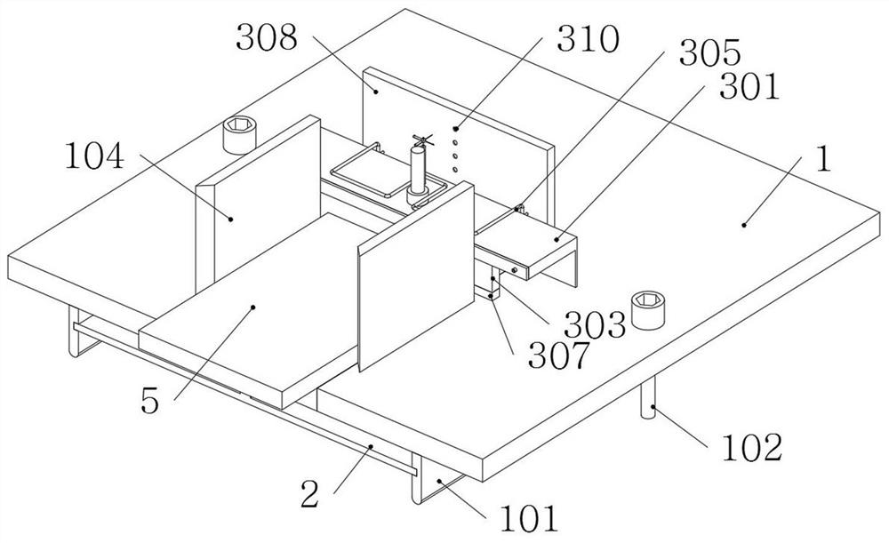
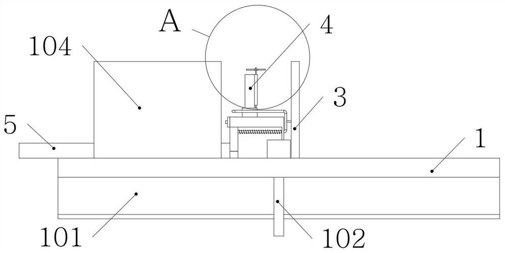
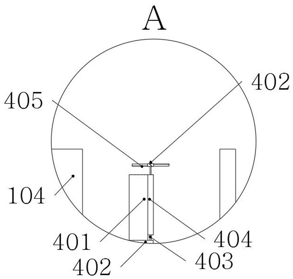
[0046] The invention provides a selective testing device for the research and development of semiconductor device materials, which includes a main body plate 1; the main body plate 1 is fixed on a workbench, and a mounting seat 2 is installed on the main body plate 1, and a blank 5 is placed on the mounting seat 2; the main body An auxiliary part 3 is installed on the board 1, and a test part 4 is installed on the auxiliary part 3; the auxiliary part 3 includes: a seat body 301, which is fixedly connected to the main body plate 1 by bolts, and two symmetrical openings are arranged on the seat body 301. Bar sliding groove 302, and two sliding grooves 302 are T-shaped groove-shaped structures; Sliding block 303, sliding block 303 is rectangular block structure, and sliding block 303 contacts with blank 5, and two Protrusion 304; two protrusions 304 are slidingly connected with two sliding grooves 302, and the sliding blo...


PUM


Abstract

The invention provides a selective testing device for semiconductor device material research and development, relates to the technical field of semiconductor testing, and solves the problems that although the conductive state of a semiconductor material can be tested through contact between the semiconductor material and a testing circuit, the structure is too single and multiple cleaning of an indicating lamp and wiping cleaning of a contact chip cannot be automatically realized in a semiconductor conduction test process through structural improvement. The selective testing device for semiconductor device material research and development comprises a main body plate. The main body plate is fixed to the workbench, a mounting base is mounted on the main body plate, and a blank is placed on the mounting base. The number of clamping grooves is two, and the two clamping grooves are formed in the two supporting plates correspondingly. The two clamping grooves are each of a rectangular groove-shaped structure, the mounting base is jointly inserted into the two clamping grooves, and after the fixing bolt is screwed down, the mounting base is in a clamped and fixed state, so that the mounting base does not need to be fixed by independently using a bolt.

Description

technical field [0001] The invention belongs to the technical field of semiconductor testing, and more specifically relates to a selection testing device for research and development of semiconductor device materials. Background technique [0002] In the process of research and development of semiconductor materials, it is necessary to conduct electrical tests on multiple semiconductor materials to test their electrical conductivity. [0003] Such as the application number: CN201410606182.7, a semiconductor test fixture, including: a base; a number of test pins located on the base, each test pin includes a first test pin, the first test pin includes a first body, located on the second A first test terminal at one end of the body and a first connection terminal at the other end of the first body; an insulator covering the surface of the first body of the first test pin; a second test terminal on the surface of the insulator surrounding the first test pin The second test need...

Claims


Application Information

Patent Timeline
Patent Type & Authority Applications(China)
IPC IPC(8): G01R1/02G01R1/04B08B1/04B08B1/00B08B5/02B08B13/00
CPCG01R1/02G01R1/04B08B1/04B08B1/006B08B5/02B08B13/00
Inventor 许海渐王海荣王磊
Owner 南通优睿半导体有限公司
Why Eureka
Try Eureka