Miniature light emitting diode display device

A technology of light-emitting diodes and display devices, which is applied in the direction of electrical components, electric solid devices, circuits, etc., can solve the problems of low process tolerance and affect the process pass rate of display devices, and achieve high process pass rate, uniform brightness, and reduce power consumption. consumption effect

Pending Publication Date: 2021-11-19
PLAYNITRIDE DISPLAY CO LTD
View PDF0 Cites 1 Cited by
  • Summary
  • Abstract
  • Description
  • Claims
  • Application Information

AI Technical Summary

Problems solved by technology

However, under the requirements of high-resolution (high PPI, such as UHD, AR / VR) display devices, the process tolerance of making metal grids in the semiconductor layer of relatively small micro light-emitting diodes will be lower, which directly affects the display performance. Process qualification rate of the device

Method used


Image

  • Miniature light emitting diode display device
  • Miniature light emitting diode display device
  • Miniature light emitting diode display device

Examples


Embodiment Construction

[0029] The micro LED display device according to some embodiments of the present invention will be described below with reference to the accompanying drawings, wherein the same elements will be described with the same reference symbols.

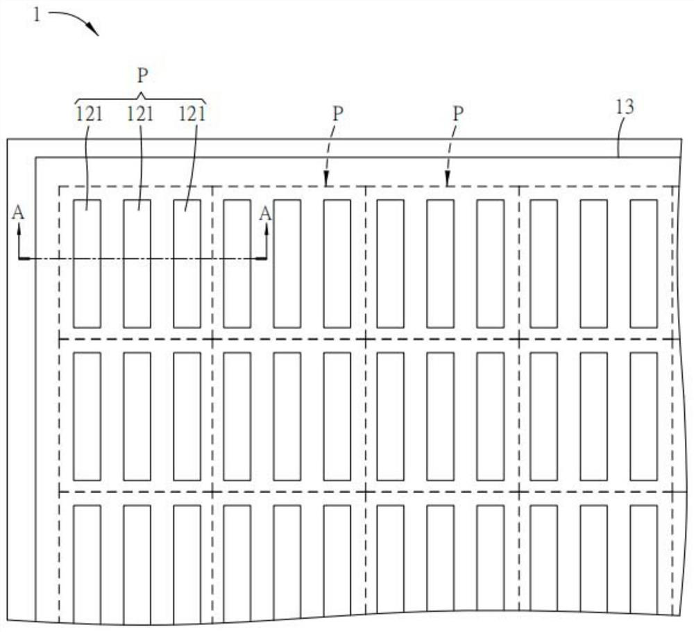
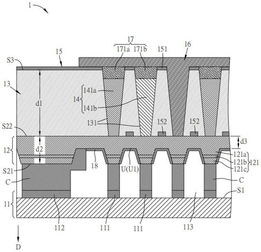
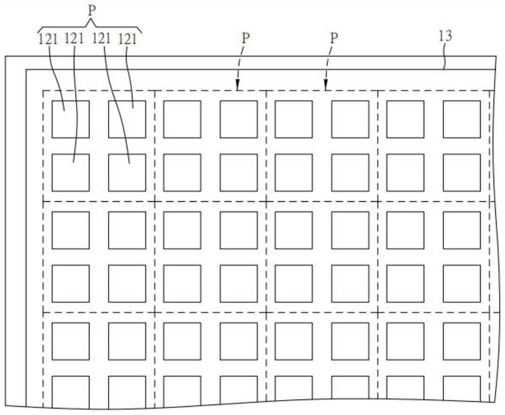
[0030] Figure 1A It is a schematic diagram of a micro light-emitting diode display device according to an embodiment of the present invention; Figure 1B for Figure 1A In the micro light-emitting diode display device of , the cross-sectional view along the section line A-A; Figure 1C It is a schematic diagram of a micro LED display device according to another embodiment of the present invention.

[0031] Figure 1A and Figure 1C The illustrated micro-LED display device 1 includes a plurality of pixels (Pixel) P, and the pixels P are arranged in a matrix formed by rows and columns. like Figure 1A As shown, each pixel P in this embodiment includes three sub-pixels (Sub-pixel) arranged side by side, and each sub-pixel includes a micro LED...


PUM

PropertyMeasurementUnit
thicknessaaaaaaaaaa
densityaaaaaaaaaa
densityaaaaaaaaaa

Abstract

The invention discloses a miniature light emitting diode display device which comprises a circuit substrate, an epitaxial structure layer, a metal conductive layer, a light conversion layer and a shading structure. The epitaxial structure layer comprises a first surface facing the circuit substrate, a second surface far away from the circuit substrate, and a plurality of micro light emitting diode units arranged at intervals, and the micro light emitting diode units are electrically connected with the circuit substrate. The metal conductive layer is arranged on the second surface and is in direct contact with the epitaxial structure layer. Each light conversion area of the metal conductive layer corresponds to one of the miniature light emitting diode units. The light conversion layer is arranged in part of the light conversion areas. The light shielding structure does not cover the light conversion areas. The thickness of the metal conductive layer is greater than the thickness of the epitaxial structure layer in the direction perpendicular to the bonding surface of the linear substrate.

Description

technical field [0001] When the world is paying attention to the future display technology, micro light emitting diode (Micro LED) is one of the most promising technologies. To put it simply, Micro LED is a technology that miniaturizes and matrixes LEDs. Millions or even tens of millions of grains smaller than 100 microns and thinner than a hair are neatly arranged on the substrate. Compared with the current OLED (Organic Light Emitting Diode) display technology, Micro LED also emits light independently, but due to the use of different materials, it can solve the most fatal "burn-in" problem of OLED, and also has low power consumption, high contrast, Wide color gamut, high brightness, small size, light and thin, energy-saving and other advantages. Therefore, major manufacturers around the world are rushing to invest in the research and development of Micro LED technology. Background technique [0002] When the world is paying attention to the future display technology, mic...

Claims


Application Information

Patent Timeline
Patent Type & Authority Applications(China)
IPC IPC(8): H01L33/62H01L27/15
CPCH01L33/62H01L27/156
Inventor 陈彦烨孙圣渊
Owner PLAYNITRIDE DISPLAY CO LTD
Why Eureka
Try Eureka