Array substrate and display panel

An array substrate and electrical connection technology, which is applied in the field of array substrates and display panels, can solve problems such as poor bright spots of display panels and inability to effectively turn off drive transistors, and achieve the effect of avoiding bad bright spots

Pending Publication Date: 2021-11-30
WUHAN CHINA STAR OPTOELECTRONICS SEMICON DISPLAY TECH CO LTD
View PDF8 Cites 1 Cited by
  • Summary
  • Abstract
  • Description
  • Claims
  • Application Information

AI Technical Summary

Problems solved by technology

[0004] The embodiment of the present application provides an array substrate and a display panel, which can solve the problem that the reset signal of the anode and the gate of the drive transistor rises at the same time in the high brightness mode, resulting in that the drive transistor cannot be effectively turned off in a black screen or a low grayscale screen. , and then the display panel has different degrees of poor bright spots

Method used


Image

  • Array substrate and display panel
  • Array substrate and display panel
  • Array substrate and display panel

Examples


Embodiment 1

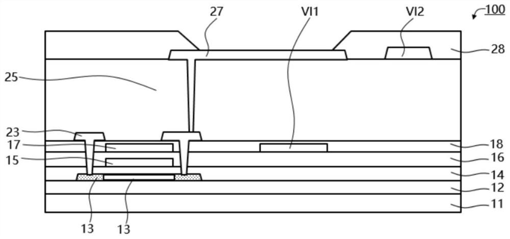
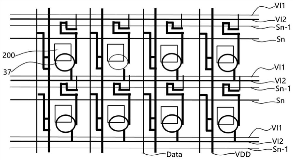
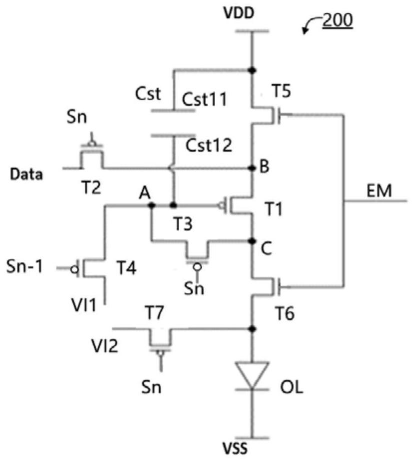
[0039] see figure 1 , figure 2 , image 3 , Figure 4 , figure 1 A schematic diagram of the film layer structure of the array substrate provided in the embodiment of the present application, figure 2 A schematic top view of the wiring connection relationship on the array substrate provided by the embodiment of the present application, image 3 A schematic diagram of an equivalent circuit of a pixel circuit on an array substrate provided in an embodiment of the present application, Figure 4 It is a schematic plan view of the arrangement of the second reset line on the array substrate provided by the embodiment of the present application.

[0040] The embodiment of the present application provides an array substrate 100, including a plurality of light-emitting elements OL arranged in an array and a pixel circuit 200 for driving the light-emitting elements OL to emit light. The first electrode of the light-emitting element OL is electrically connected to the first power s...

Embodiment 2

[0049] The embodiment of the present application is based on the first embodiment, and further illustrates the film layer structure in the above embodiment.

[0050] The array substrate 100 includes a stacked substrate 11, a second metal layer 17, and a first metal layer 27. The first metal layer 27 includes the first electrode of the light emitting element OL, and the wiring of the first reset signal source VI1 and the second reset signal source VI1. One of the wires of the signal source VI2, the second metal layer 17 includes the wires of the first reset signal source VI1 and the other of the wires of the second reset signal source VI2.

[0051] Specifically, the first metal layer 27 includes the first electrode of the light emitting element OL and the wiring of the first reset signal source VI1, and the second metal layer 17 includes the wiring of the second reset signal source VI2.

[0052] Specifically, the first metal layer 27 includes the first electrode of the light em...

Embodiment 3

[0056] The embodiments of the present application are based on the foregoing embodiments, and further illustrate the structures in the foregoing embodiments.

[0057] In some embodiments, the pixel circuit 200 further includes a compensation transistor T3, the gate of the compensation transistor T3 is electrically connected to the first scan line Sn, the source of the compensation transistor T3 is electrically connected to the third node C, and the drain of the compensation transistor T3 is electrically connected to The first node A.

[0058] In some embodiments, the pixel circuit 200 further includes a first light emission control transistor T5 and a second light emission control transistor T6, the gate of the first light emission control transistor T5 is electrically connected to the light emission control signal line EM, and the source of the first light emission control transistor T5 The pole is electrically connected to the first power supply VDD, the drain of the first l...


PUM


Abstract

The embodiment of the invention discloses an array substrate and a display panel, and the array substrate comprises a plurality of light-emitting elements arranged in an array and a pixel circuit for driving the light-emitting elements to emit light; the pixel circuit comprises a driving transistor, a data writing transistor, a storage capacitor, a reset transistor and a reset transistor; a gate electrode of the reset transistor is electrically connected with a second scanning line, a source electrode of the reset transistor is electrically connected with the first node, and a drain electrode of the reset transistor is electrically connected with a first reset signal source; the gate electrode of the reset transistor is electrically connected with the first scanning line, the source electrode of the reset transistor is electrically connected with a second reset signal source, and the drain electrode of the reset transistor is connected to the first electrode of the light-emitting element. According to the embodiment of the invention, the reset signals of the grid electrode and the anode of the driving transistor in the highlight mode can be prevented from rising at the same time, so that the driving transistor can be effectively closed in a black picture or a low-gray-scale picture, and the display panel is prevented from having different degrees of poor bright spots.

Description

technical field [0001] The present application relates to the display field, in particular to an array substrate and a display panel. Background technique [0002] As OLED panels (organic light-emitting display panels) are widely used, the usage environments are also gradually increasing. The requirements for the maximum brightness and power consumption of the screen are getting higher and higher. In order to meet the needs of outdoor personnel, the current screens will increase the brightness of the HBM (High brightness mode) to achieve the purpose. In order to increase the brightness of HBM, the current main solution is to increase the reset voltage of the anode, thereby reducing the charging time required for the anode to reach the turn-on voltage, so as to increase the luminous time at the same refresh rate to increase the brightness. [0003] However, at present, the anode and the gate of the drive transistor are electrically connected to the same reset signal, increa...

Claims


Application Information

Patent Timeline
Patent Type & Authority Applications(China)
IPC IPC(8): G09G3/3208
CPCG09G3/3208
Inventor 王傲
Owner WUHAN CHINA STAR OPTOELECTRONICS SEMICON DISPLAY TECH CO LTD
Why Eureka
Try Eureka