Double-flash mainboard, electronic equipment applying same and design method of double-flash mainboard

A technology of electronic equipment and design method, applied in dual flash motherboards, electronic equipment and design fields, can solve the problems of device placement and wiring layout difficulty, and achieve reduced wiring difficulty, optimized space, and broad application prospects Effect

Inactive Publication Date: 2021-12-17
INSPUR SUZHOU INTELLIGENT TECH CO LTD
View PDF0 Cites 1 Cited by
  • Summary
  • Abstract
  • Description
  • Claims
  • Application Information

AI Technical Summary

Problems solved by technology

[0005] The invention provides a dual-flash motherboard, electronic equipment using the same and a design method thereof, which are used to solve the problem of difficulty in device placement and wiring layout in the existing motherboard architecture

Method used


Image

  • Double-flash mainboard, electronic equipment applying same and design method of double-flash mainboard
  • Double-flash mainboard, electronic equipment applying same and design method of double-flash mainboard
  • Double-flash mainboard, electronic equipment applying same and design method of double-flash mainboard

Examples


Embodiment Construction

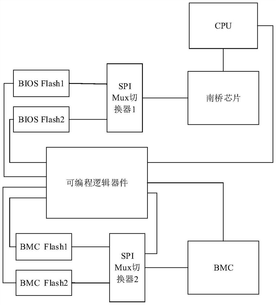
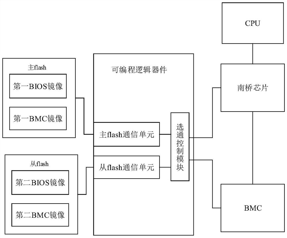
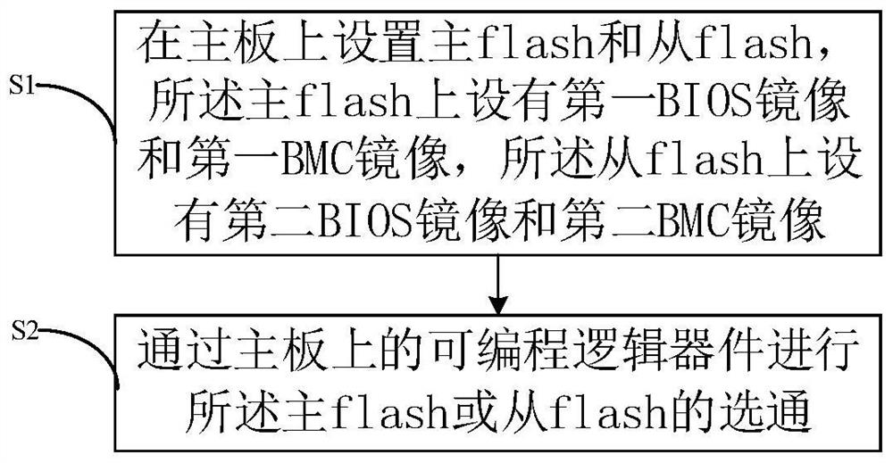
[0030] In order to clearly illustrate the technical features of this solution, the present invention will be described in detail below through specific implementation modes and in conjunction with the accompanying drawings. The following disclosure provides many different embodiments or examples for implementing different structures of the present invention. To simplify the disclosure of the present invention, components and arrangements of specific examples are described below. Furthermore, the present invention may repeat reference numerals and / or letters in different instances. This repetition is for the purpose of simplicity and clarity and does not in itself indicate a relationship between the various embodiments and / or arrangements discussed. It should be noted that components illustrated in the figures are not necessarily drawn to scale. Descriptions of well-known components and processing techniques and processes are omitted herein to avoid unnecessarily limiting the...


PUM


Abstract

The invention provides a double-flash mainboard, electronic equipment applying the same and a design method of the double-flash mainboard, the double-flash mainboard comprises a programmable logic device, the mainboard further comprises a master flash and a slave flash, the master flash is provided with a first BIOS mirror image and a first BMC mirror image, and the slave flash is provided with a second BIOS mirror image and a second BMC mirror image; and the programmable logic device is used for gating of the master flash and the slave flash. According to the invention, the main flash and the slave flash are arranged on the mainboard, and each flash is provided with the BIOS mirror image and the BMC mirror image, so that the requirement of double flashes of devices on the mainboard is met, the requirement can be realized by arranging only two flashes on the mainboard, and the number of the devices on the mainboard is reduced; in addition, the gating function of the master flash and the slave flash is integrated into the programmable logic device, so that the number of devices on the mainboard is further reduced. The number of solid parts on the mainboard is reduced, the space of circuit layout is optimized, the wiring difficulty is reduced, and the placing elasticity of the parts is improved.

Description

technical field [0001] The invention relates to the technical field of server motherboard design, in particular to a dual-flash motherboard, electronic equipment using the same and a design method thereof. Background technique [0002] When designing the current motherboard, it is necessary to reserve dual flash (a type of memory device, which is a non-volatile memory) to deal with the situation that the system cannot operate normally due to flash damage. [0003] For the motherboard, such as figure 1 As shown, the objects that need to reserve dual flash devices include BIOS (Basic Input Output System, Basic Input Output System) and BMC (Baseboard Management Controller, Baseboard Management Controller), so four flash chips need to be set on one motherboard. And for the gate switching of the two flashes, a corresponding SPI (Serial Peripheral Interface, Serial Peripheral Interface) MUX (multiplexer, transfer switch) switcher is required to realize. [0004] In the design st...

Claims


Application Information

Patent Timeline
Patent Type & Authority Applications(China)
IPC IPC(8): G06F1/18G06F11/14G06F13/16
CPCG06F1/184G06F11/1402G06F13/1657
Inventor 张志玮
Owner INSPUR SUZHOU INTELLIGENT TECH CO LTD
Why Eureka
Try Eureka