Driving system and method of touch display panel

A touch display panel and drive system technology, applied in the direction of static indicators, instruments, etc., can solve the problems of large coupling amount, pixel difference of touch display panel, difference of coupling amount of common electrode layer, etc.

Pending Publication Date: 2022-01-07
FOCALTECH ELECTRONICS
View PDF11 Cites 0 Cited by
  • Summary
  • Abstract
  • Description
  • Claims
  • Application Information

AI Technical Summary

Problems solved by technology

[0002] The structure of the existing in-cell touch display panel is to cut the common electrode layer (VCOM) which was originally covered by the whole layer into multiple touch electrodes, such as figure 1 As shown, because the above-mentioned cutting of the common electrode layer is a plurality of touch electrodes 11, it will inevitably cause the original full coverage of the common electrode layer to be cut to form an area not covered by the common electrode layer, which will cause touch display. The difference in the load of the pixels of the panel, when driving the gate lines (Gate Lines), the gate lines not covered by the common electrode layer (such as G[i]), and the gate lines still covered by the common electrode layer ( For example, G[i-1], G[i+1], etc.) will produce different coupling amounts, resulting in differences in the amount of coupling between the divided common electrode layers, and then forming the phenomenon of Mura
Especially for the GOA (Gate driver On Array) touch display panel, due to the long output width of the gate driving voltage of the gate line, the amount of coupling to the common electrode layer of the panel in the adjacent gate line is relatively large, Therefore, when encountering an area that does not cover the common electrode layer, it is easier to cause differences in display from other areas that cover the common electrode layer
[0003] Therefore, the current touch display panel design cannot avoid the horizontal stripes caused by cutting the common electrode layer into multiple touch electrodes, and it is necessary to improve it.

Method used


Image

  • Driving system and method of touch display panel
  • Driving system and method of touch display panel
  • Driving system and method of touch display panel

Examples


Embodiment Construction

[0024] In order to make the object, technical solution and advantages of the present invention clearer, the present invention will be further described in detail below in conjunction with the accompanying drawings and embodiments. It should be understood that the specific embodiments described here are only used to explain the embodiments of the present invention, and are not intended to limit the present invention.

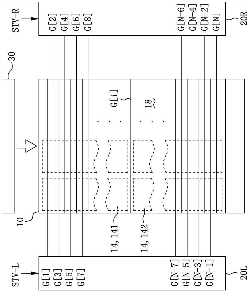
[0025] figure 2 The driving system of the touch display panel of the present invention is schematically shown, which includes a panel 10 , a left gate driving circuit 20L, a right gate driving circuit 20R, and a source driving circuit 30 . The panel 10 is, for example, a touch display panel, and the panel 10 has an active area 18 for display or touch. The left gate driving circuit 20L is arranged on the left side of the active region 18 of the panel 10, the right gate driving circuit 20R is arranged on the right side of the active region 18 of the panel 10, the...


PUM


Abstract

The invention discloses a driving system of a touch display panel. The driving system comprises a panel, a left side gate drive circuit and a right side gate drive circuit, the panel is provided with an active area; the left side gate drive circuit is arranged on the left side of the active area of the panel and connected with a plurality of left side gate lines so as to provide gate driving voltage for driving in a scanning direction; the right gate drive circuit is arranged on the right side of the active area of the panel and connected with the right gate lines so as to provide gate driving voltage for driving in a scanning direction, and the scanning direction of driving of the left gate drive circuit is opposite to the scanning direction of driving of the right gate drive circuit. Driving is carried out in different scanning directions through the grid drive circuit, and transverse lines caused by layout gaps of the touch electrodes can be avoided.

Description

technical field [0001] The present invention relates to a driving system and method of a touch display panel, in particular to a driving system and method of a touch display panel capable of avoiding horizontal stripes caused by gaps between touch point electrodes. Background technique [0002] The structure of the existing in-cell touch display panel is to cut the common electrode layer (VCOM) which was originally covered by the whole layer into multiple touch electrodes, such as figure 1 As shown, because the above-mentioned cutting of the common electrode layer is a plurality of touch electrodes 11, it will inevitably cause the original full coverage of the common electrode layer to be cut to form an area not covered by the common electrode layer, which will cause touch display. The difference in the load of the pixels of the panel, when driving the gate lines (Gate Lines), the gate lines not covered by the common electrode layer (such as G[i]), and the gate lines still c...

Claims


Application Information

Patent Timeline
Patent Type & Authority Applications(China)
IPC IPC(8): G09G3/20
CPCG09G3/20
Inventor 陈奕冏洪瑞隆郑建豪施博盛
Owner FOCALTECH ELECTRONICS
Why Eureka
Try Eureka