Array substrate and display panel

A technology for array substrates and opposing substrates, applied in the field of array substrates and display panels, can solve the problems of GatelineGN waveform differences, easy increase in lateral capacitance, resistance and capacitance differences, etc., to solve the problem of different lateral capacitances, improve bright and dark lines, The effect of consistent overall length

Active Publication Date: 2022-01-21
SHENZHEN CHINA STAR OPTOELECTRONICS SEMICON DISPLAY TECH CO LTD
View PDF1 Cites 2 Cited by
  • Summary
  • Abstract
  • Description
  • Claims
  • Application Information

AI Technical Summary

Problems solved by technology

Therefore, there are differences in the resistance and capacitance between CK1~8, which will lead to differences in the GN waveforms of two adjacent rows of Gatelines
Because of the difference in the resistance and capacitance of adjacent CK wires, there are differences in the scanning signal waveforms output by two adjacent rows of Gatelines, resulting in significant differences in brightness due to charging differences, which in turn causes periodic horizontal dense lines to appear on the product.
[0004] During the research and practice of the prior art, the inventor of the present application found that in the actual product design, the compensation and matching of capacitance and resistance will be carried out by means of winding, but the existing winding compensation method is easy to increase The presence of lateral capacitance

Method used


Image

  • Array substrate and display panel
  • Array substrate and display panel
  • Array substrate and display panel

Examples


Embodiment Construction

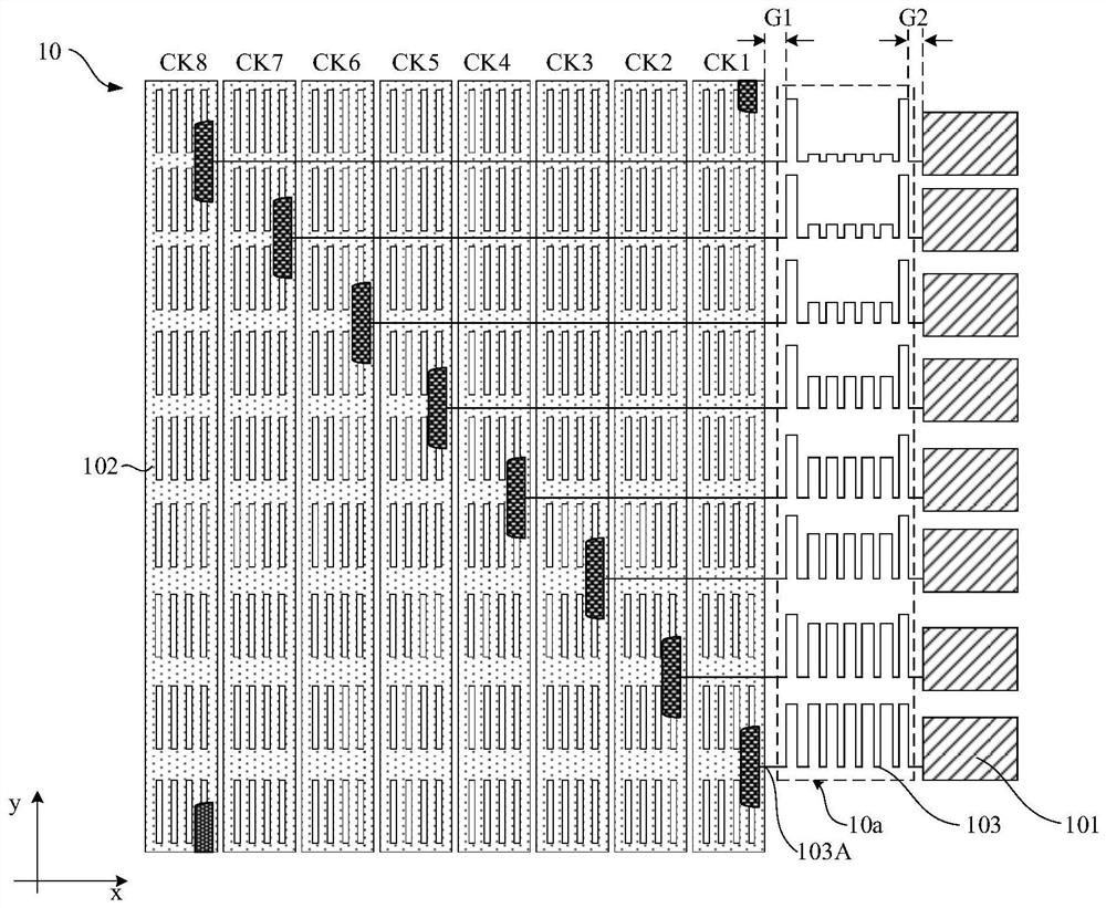
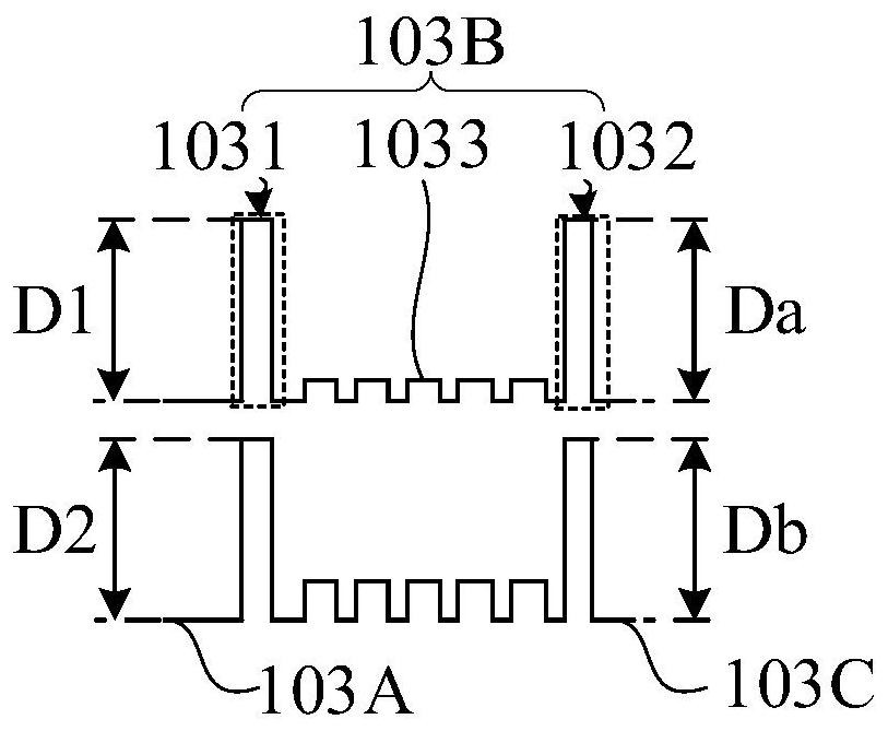
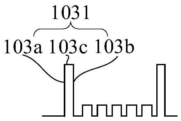
[0041] The following will clearly and completely describe the technical solutions in the embodiments of the application with reference to the drawings in the embodiments of the application. Apparently, the described embodiments are only some of the embodiments of the application, not all of them. Based on the embodiments in this application, all other embodiments obtained by those skilled in the art without making creative efforts belong to the scope of protection of this application. In addition, it should be understood that the specific implementations described here are only used to illustrate and explain the present application, and are not intended to limit the present application. In this application, unless stated to the contrary, the used orientation words such as "up" and "down" usually refer to up and down in the actual use or working state of the device, specifically the direction of the drawing in the drawings ; while "inside" and "outside" refer to the outline of ...


PUM


Abstract

Embodiments of the invention disclose an array substrate and a display panel. The array substrate provided by one embodiment of the invention comprises a plurality of GOA units, a plurality of clock signal lines and a plurality of communication lines, wherein the lengths of the plurality of communication lines are the same; a winding area is arranged between the clock signal lines and the GOA units; the communication lines are bent in the winding area; and in the winding area, the lateral capacitance of the communication lines close to the clock signal lines or close to at least one sides of the GOA units is the same. Through the above winding design, lateral capacitance matching of the communication line on the same side can be consistent. Therefore, the problem that lateral capacitance generated by communication lines in different rows and surrounding wires is different is solved. Besides, the communication lines are subjected to winding design in the winding area, so the total lengths of the communication lines in different rows are consistent, the problem that the resistance and capacitance of the communication lines in different rows are inconsistent is solved, and the problem of light and dark lines of a panel can be solved.

Description

technical field [0001] The present application relates to the field of display technology, in particular to an array substrate and a display panel. Background technique [0002] In panel products, the normal display of the active area (AA) is jointly controlled by the scan line (Gateline) and the data line (Dataline). The voltage signal required by the pixel. [0003] In GOA products, the Gateline signal is transmitted from the bus (Busline) to the gate drive unit (GOACircuit), and then input to the Gateline wiring in the AA area through the GOA Circuit. Usually the CKs in the Busline are sorted from the inside to the outside. Taking 8 clock signals as an example, CK8 at the outermost edge needs to cross CK7-CK1 to connect to the GOA unit, and CK1 does not need to cross other CKs. Therefore, there are differences in the resistance and capacitance between CK1-8, which in turn leads to differences in the GN waveforms of two adjacent rows of Gatelines. Because of the differ...

Claims


Application Information

Patent Timeline
Patent Type & Authority Applications(China)
IPC IPC(8): H01L27/12
CPCH01L27/1214H01L27/124
Inventor 陈志祥王添鸿
Owner SHENZHEN CHINA STAR OPTOELECTRONICS SEMICON DISPLAY TECH CO LTD
Why Eureka
Try Eureka