
Scalable integrated circuit with synaptic electronics and CMOS integrated memristors

A circuit and synapse technology, applied in the field of neural networks, which can solve the problem that the connection is not programmable.

Pending Publication Date: 2022-01-28
HRL LAB
View PDF4 Cites 1 Cited by
  • Summary
  • Abstract
  • Description
  • Claims
  • Application Information

AI Technical Summary

Problems solved by technology

However, in this circuit, the connection is not programmable

Method used


Image

  • Scalable integrated circuit with synaptic electronics and CMOS integrated memristors
  • Scalable integrated circuit with synaptic electronics and CMOS integrated memristors
  • Scalable integrated circuit with synaptic electronics and CMOS integrated memristors

Examples


Embodiment Construction

[0032] In the following description, numerous specific details are set forth in order to clearly describe various specific embodiments disclosed herein. However, it will be understood by those skilled in the art that the present invention may be practiced without all of the specific details discussed below. In other instances, well-known features have not been described in order not to obscure the invention.

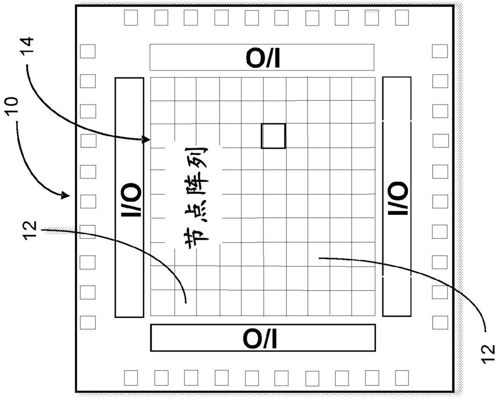
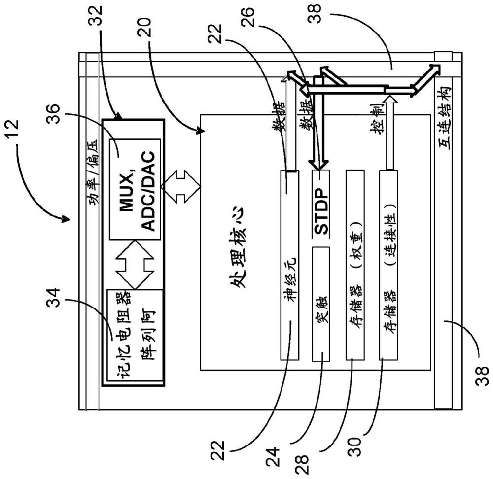
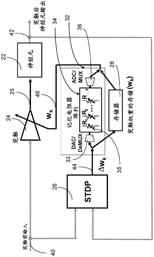
[0033] In this disclosure, scalable neuromorphic integrated circuits with spiking neurons, synapses, and spike timing-dependent plasticity (STDP) are described, where connections between neurons and synapses are not fixed but can be programmed of. Synapses, STDP circuits, and interconnection paths between neurons and synapses are time multiplexed. The integrated circuit includes memory that stores synaptic weights and interconnect routing information. Circuitry includes CMOS circuitry to implement high-density memristor memory and write and read memristors.

[0034] ...


PUM


Abstract

A reconfigurable neural circuit includes an array of processing nodes. Each processing node includes a single physical neuron circuit having only one input and an output, a single physical synapse circuit having a presynaptic input, and a single physical output coupled to the input of the neuron circuit, a weight memory for storing N synaptic conductance value or weights having an output coupled to the single physical synapse circuit, a single physical spike timing dependent plasticity (STDP) circuit having an output coupled to the weight memory, a first input coupled to the output of the neuron circuit, and a second input coupled to the presynaptic input, and interconnect circuitry connected to the presynaptic input and connected to the output of the single physical neuron circuit. The synapse circuit and the STOP circuit are each time multiplexed circuits. The interconnect circuitry in each respective processing node is coupled to the interconnect circuitry in each other processing node.

Description

[0001] Cross References to Related Applications [0002] This application relates to and claims priority to U.S. Patent Application Serial No. 16 / 447,210, filed June 20, 2019, which is a continuation-in-part of U.S. Patent Application Serial No. 14 / 453,154, filed August 6, 2014, and relates to and Priority is claimed to U.S. Provisional Application No. 61 / 890,166, filed October 11, 2013, and U.S. Provisional Application No. 61 / 890,790, filed October 14, 2013, which are incorporated herein as if The full text is the same. This application is also related to U.S. Application No. 13 / 415,812 filed March 8, 2012, U.S. Application No. 13 / 535,114 filed June 27, 2012, and U.S. Patent Application No. 13 / 679,727, these applications are incorporated herein as if set forth in full. [0003] Statement Regarding Federal Funding [0004] This invention was made under US Government contract HR0011-09-C-0001. The US Government has certain rights in this invention. technical field [0005...

Claims


Application Information

Patent Timeline
Patent Type & Authority Applications(China)
IPC IPC(8): G06N3/04G06N3/063G06N3/08G11C11/54G11C11/56G11C13/00
CPCG06N3/049G11C13/0007G11C13/0023G06N3/088G11C11/5685G11C11/54G06N3/065
Inventor 乔斯·克鲁兹-阿尔布雷克特蒂莫西·德罗西耶纳拉扬·斯里尼瓦萨
Owner HRL LAB
Learn More