Semiconductor device and electronic device

a semiconductor and electronic technology, applied in the field of semiconductor devices, can solve the problems of increasing chip area, power consumption, and difficult data retention time, and achieve the effects of reducing power consumption, reducing chip area, and reducing complexity

Active Publication Date: 2017-04-27
SEMICON ENERGY LAB CO LTD
View PDF0 Cites 34 Cited by
  • Summary
  • Abstract
  • Description
  • Claims
  • Application Information

AI Technical Summary

Benefits of technology

[0017]Alternatively, an object of one embodiment of the present invention is to provide a semiconductor device or the like with a novel configuration and a reduced chip area. Another object of one embodiment of the present invention is to provide a semiconductor device or the like with a novel configuration, in which power consumption is reduced. Another object of one embodiment of the present invention is to provide a semiconductor device or the like with a novel configuration, in which the hierarchical structure constituting of circuits such as the neuron circuit or the synapse circuit can be freely changed.
[0023]One embodiment of the present invention can provide a novel semiconductor device, a novel display device, a novel electronic device, or the like.
[0024]One embodiment of the present invention can provide a semiconductor device or the like with a novel configuration and a reduced chip area. Another embodiment of the present invention can provide a semiconductor device or the like with a novel configuration, in which power consumption is reduced. Another embodiment of the present invention can provide a semiconductor device or the like with a novel configuration, in which the hierarchical structure constituting of circuits such as the neuron circuit or the synapse circuit can be freely changed.

Problems solved by technology

However, configuring an analog memory that is ideal for the above memory, that is, an analog memory capable of storing analog values, is highly difficult.
In the case where the analog memory cell with a dynamic random access memory (DRAM) type cell structure is used, the data retention time is extremely short.
The configurations, however, increases in a chip area, and power consumption.

Method used


Image

  • Semiconductor device and electronic device
  • Semiconductor device and electronic device
  • Semiconductor device and electronic device

Examples


embodiment 1

[0063]The embodiment of the present invention is explained with reference to FIG. 1, FIGS. 2A to 2D, FIG. 3, FIG. 4, FIG. 5, FIG. 6, FIG. 7, FIG. 8, and FIG. 9.

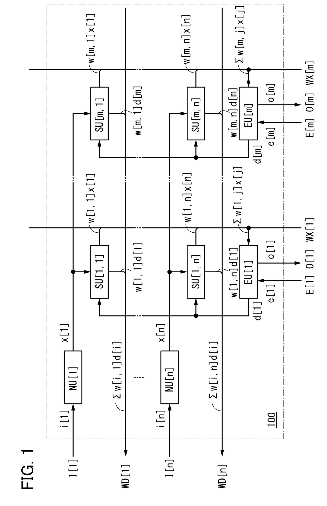
[0064]FIG. 1 shows circuit blocks of module 100 that make up the semiconductor device. Module 100 is made up of n (n is a natural number) neuron circuits NU, m×n (m is a natural number) synapse circuits SU, and m error circuits EU.

[0065]Each of the circuit blocks that make up the module 100 illustrated in FIG. 1 is explained below.

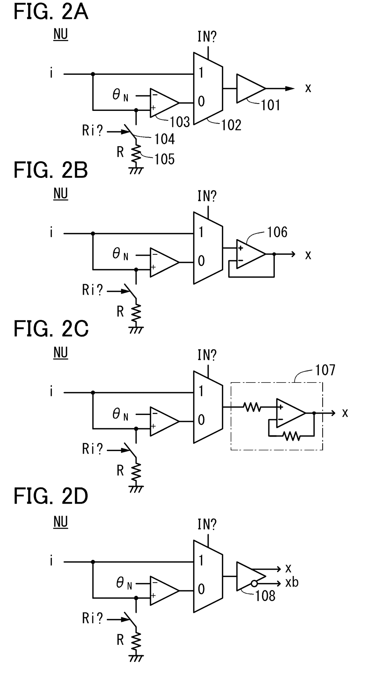
[0066]FIG. 2A illustrates a configuration of the neuron circuit NU. The neuron circuit NU can function as an input neuron circuit or as a hidden neuron circuit. The neuron circuit NU includes an amplifier 101, a selector circuit 102, a differential amplifier 103, a switch 104 and a resistor 105.

[0067]When the neuron circuit NU is to function as the input neuron circuit, the signal to be output is changed to the side of “1” by a switching signal (IN? in FIGS. 2A to 2D) of the selector circuit 102. Th...

embodiment 2

[0125]In this embodiment, an operation example of the semiconductor device illustrated in FIG. 1 is described. Here, an operation of a three-layer neural network with modules 10013 1 and 10013 2 illustrated in FIG. 33 is described as an operation of the semiconductor device. The selector circuit is set so that the neuron circuit NU of the first module 100_1 is the input neuron circuit, the error circuit EU of the first module 100_1 is the hidden error circuit, the neuron circuit NU of the second module 100_2 is the hidden neuron circuit, and the error circuit EU of the second module 100_2 is the output neuron circuit. The output signal of the synapse circuit SU of the first module 100_1 serves as the input signal of the neuron circuit NU of the second module 100_2, and the error signal from the synapse circuit SU of the second module 100_2 serves as the input signal of the error circuit EU of the first module 100_1.

[0126]The operation of the semiconductor device refers to an operati...

embodiment 3

[0151]In this embodiment, an operation example where the semiconductor device described in Embodiment 1 and illustrated in FIG. 1 is used as an encoder is described.

[0152]Firstly, an example of detecting a motion of an object is described. FIGS. 12A to 12F illustrate an algorithm performed by the encoder on image data for detection of the motion of the object.

[0153]FIG. 12A shows image data 10 that has a triangle 11 and a circle 12. FIG. 12B shows image data 20 where the triangle 11 and the circle 12 of the image data 10 are moved to the upper right.

[0154]Image data 30 in FIG. 12C shows an operation by which a region 31 including the triangle 11 and the circle 12 is extracted from the image data 10. In the image data 30, a cell at the upper left corner of the extracted region 31 is regarded as a reference point (0, 0), and numbers indicating positions in the right / left and upper / lower directions are added to the image data 10. The extracted region 31 of FIG. 12C is shown in FIG. 12E...


PUM


Abstract

A neuron circuit can switch between two functions: as an input neuron circuit, and as a hidden neuron circuit. An error circuit can switch between two functions: as a hidden error circuit, and as an output neuron circuit. A switching circuit is configured to be capable of changing the connections between the neuron circuit, a synapse circuit, and the error circuit. The synapse circuit includes an analog memory that stores data that corresponds to the connection strength between the input neuron circuit and the hidden neuron circuit or between the hidden neuron circuit and the output neuron circuit, a writing circuit that changes the data in the analog memory, and a weighting circuit that weights an input signal in reaction to the data of the analog memory and outputs the weighted output signal. The analog memory includes a transistor comprising an oxide semiconductor with extremely low off-state current.

Description

TECHNICAL FIELD[0001]One embodiment of the present invention relates to an electronic device which includes a semiconductor device or the semiconductor device.[0002]Note that one embodiment of the present invention is not limited to the above technical field. The technical field of the invention disclosed in this specification and the like relates to an object, a method, or a manufacturing method. Furthermore, one embodiment of the present invention relates to a process, a machine, manufacture, or a composition of matter. Specifically, examples of the technical field of one embodiment of the present invention disclosed in this specification include a semiconductor device, a display device, a light-emitting device, a power storage device, a memory device, a method for driving any of them, and a method for manufacturing any of them.[0003]In this specification and the like, a semiconductor device refers to an element, a circuit, a device, or the like that can function by utilizing semi...

Claims


Application Information

Patent Timeline
Patent Type & Authority Applications(United States)
IPC IPC(8): G06N3/063G11C27/00
CPCG11C27/005G06N3/063G11C11/24G11C11/54G06N3/065
Inventor KUROKAWA, YOSHIYUKI
Owner SEMICON ENERGY LAB CO LTD
Why Eureka
Try Eureka