Optical imaging lens and imaging equipment
An optical imaging lens and imaging surface technology, applied in the field of imaging lens, can solve problems such as difficult to meet the requirements of the preview distance, reduce the target recognition range, and poor imaging effect, and achieve improved imaging performance, clear imaging, and good thermal stability Effect
- Summary
- Abstract
- Description
- Claims
- Application Information
AI Technical Summary
Problems solved by technology
Method used
Image
Examples
no. 1 example
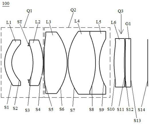
[0084] see figure 1 , is a schematic structural diagram of the optical imaging lens 100 provided in the first embodiment of the present invention, the optical imaging lens 100 includes in sequence from the object side to the imaging surface along the optical axis: a first group Q1 with negative optical power, and a first group Q1 with positive optical power The second group Q2 with positive power, the third group Q3 with positive power, and the filter G1.
[0085] The first group Q1 includes in order from the object side to the imaging plane along the optical axis: a first lens L1 and a second lens L2. The second group Q2 includes in sequence from the object side to the imaging plane along the optical axis: a third lens L3, a fourth lens L4, and a fifth lens L5. The third group Q3 sequentially includes the sixth lens L6 along the optical axis from the object side to the imaging surface. A stop ST is provided between the first lens L1 and the second lens L2.
[0086] Wherein...
no. 2 example
[0101] Please refer to Figure 5 , the structure of the optical imaging lens 200 in this embodiment is roughly the same as that of the optical imaging lens 100 in the first embodiment, the difference is that: the object side S10 of the sixth lens is a convex surface, and the image side S11 is a concave surface; finally The mechanical back focus between the sixth lens L6 and the imaging surface S14 of a lens is lengthened; and there are differences in the materials of some lenses, the relevant parameters of each lens and the air gap.
[0102] The relevant parameters of each lens of the optical imaging lens 200 provided in this embodiment are shown in Table 3.
[0103] table 3
[0104]
[0105] The surface coefficients of each aspheric surface in the optical imaging lens 200 in this embodiment are shown in Table 4.
[0106] Table 4
[0107]
[0108] The distortion curve diagram, MTF diagram and axial chromatic aberration diagram of the optical imaging lens 200 provided in...
no. 3 example
[0110] Please refer to Figure 9 , the structure of the optical imaging lens 300 in this embodiment is roughly the same as that of the optical imaging lens 100 in the first embodiment, the difference is that the second lens L2 adopts an aspherical lens, and the sixth lens L6 has a negative optical focus There are differences in the relevant parameters and air intervals of the lens, as well as the parameters of each lens of the lens.
[0111] The relevant parameters of each lens of the optical imaging lens 300 provided in this embodiment are shown in Table 5.
[0112] table 5
[0113]
[0114] Table 6 shows the surface coefficients of each aspheric surface of the optical imaging lens 300 in this embodiment.
[0115] Table 6
[0116]
[0117] The distortion curve diagram, MTF diagram and axial chromatic aberration diagram of the optical imaging lens 300 provided in this embodiment are respectively as follows Figure 10 , Figure 11 and Figure 12 shown. Depend on ...
PUM
 Abstract
Description
Claims
Application Information


