

Optical imaging element with magnetic reflecting layer imaging unit and preparation method thereof
An optical imaging, imaging unit technology, applied in optical components, optics, grafted polymer adhesives, etc., can solve the problem of insufficient resolution and clarity of aerial imaging, commercial promotion and large-scale application of medium-free aerial imaging technology. , affecting the user experience and other issues, to achieve the effect of low insertion loss, increased dielectric constant, and elimination of influence
- Summary
- Abstract
- Description
- Claims
- Application Information
AI Technical Summary
Problems solved by technology
Method used
Image

Examples
Embodiment 1
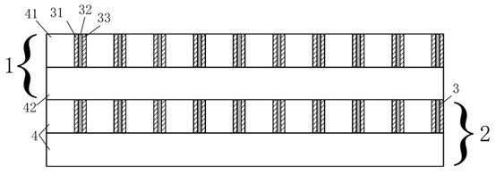
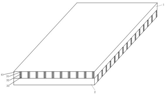
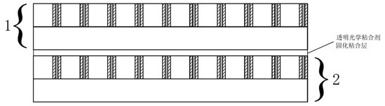
[0053] like Figure 1-2 As shown, the optical imaging element provided in this embodiment has a magnetic reflective layer imaging unit, the optical imaging element includes a superimposed optical imaging unit, and the optical imaging unit includes an upper transparent laminated body 1 and a lower transparent laminated body 2, The upper light-transmitting laminated body 1 and the lower-layer light-transmitting laminated body 2 have the same structure, and are composed of several light-transmitting strips 4 with reflective layers 3 arranged side by side. The direction of the light strip 41 is perpendicular to the direction of the second light-transmitting strip 42 in the lower light-transmitting laminated body 2;
[0054] The reflective layer 3 is a sandwich laminated metal magnetic thin layer, and the sandwich laminated metal magnetic thin layer 3 includes a first metal aluminum layer 31, a central magnetic layer 32 and a second metal aluminum layer 33, the first metal aluminum...
Embodiment 2
[0056] The optical imaging element provided in this embodiment has a magnetic reflective layer imaging unit. The optical imaging element includes two superimposed optical imaging units. The optical imaging unit includes an upper transparent laminated body 1 and a lower transparent laminated body 2. The body 1 and the lower light-transmitting laminated body 2 have the same structure, and are composed of several light-transmitting strips 4 with reflective layers 3 arranged side by side. It is characterized in that the first light-transmitting strip 41 in the upper light-transmitting laminated body set perpendicular to the direction of the second light-transmitting strip 42 in the lower light-transmitting laminated body 2;
[0057] The reflective layer 3 is a sandwich laminated metal magnetic thin layer, and the sandwich laminated metal magnetic thin layer 3 includes a first metal aluminum layer 31, a central magnetic layer 32 and a second metal aluminum layer 33, the first metal ...
Embodiment 3
[0059] This embodiment provides an optical imaging element with a magnetic reflective layer imaging unit, the optical imaging element includes 5 superposed optical imaging units, the optical imaging unit includes an upper transparent laminated body 1 and a lower transparent laminated body 2, and the upper transparent laminated body 1 and the lower light-transmitting laminated body 2 have the same structure, and are composed of several light-transmitting strips 4 with reflective layers 3 arranged side by side. The directions of the second light-transmitting strips 42 in the lower light-transmitting laminated body 2 are vertically intersecting;
[0060] The reflective layer 3 is a sandwich laminated metal magnetic thin layer, the sandwich laminated metal magnetic thin layer 3 includes a first metal aluminum layer 31, a central magnetic layer 32 and a second metal aluminum layer 33, the first metal aluminum layer 31 and the second metal aluminum layer 33 sandwich the central magn...
PUM
| Property | Measurement | Unit |
|---|---|---|
| thickness | aaaaa | aaaaa |
| thickness | aaaaa | aaaaa |
| thickness | aaaaa | aaaaa |
Abstract
Description
Claims
Application Information