
Method, device and equipment for repairing single crystal memory

A single crystal, memory technology, applied in static memory, instruments, etc., can solve the problems of waste of resources, inability to achieve good products, environmental pollution, etc., and achieve the effect of saving resources and protecting the environment.

Pending Publication Date: 2022-03-01
SHENZHEN JIAHE JINWEI ELECTRONICS TECH
View PDF0 Cites 0 Cited by
  • Summary
  • Abstract
  • Description
  • Claims
  • Application Information

AI Technical Summary

Problems solved by technology

[0003] However, memory manufacturers cannot achieve 100% good products in wafer production and IC packaging.
[0004] At present, the defective products produced by memory manufacturers are about 10-15%, resulting in a large waste of resources. Since precious metals are used in the memory IC and packaging process, if the defective products are destroyed, it will also cause further waste of resources. ; and the current extraction of precious metals by chemical methods will cause environmental pollution to a certain extent

Method used


Image

  • Method, device and equipment for repairing single crystal memory
  • Method, device and equipment for repairing single crystal memory
  • Method, device and equipment for repairing single crystal memory

Examples


Embodiment Construction

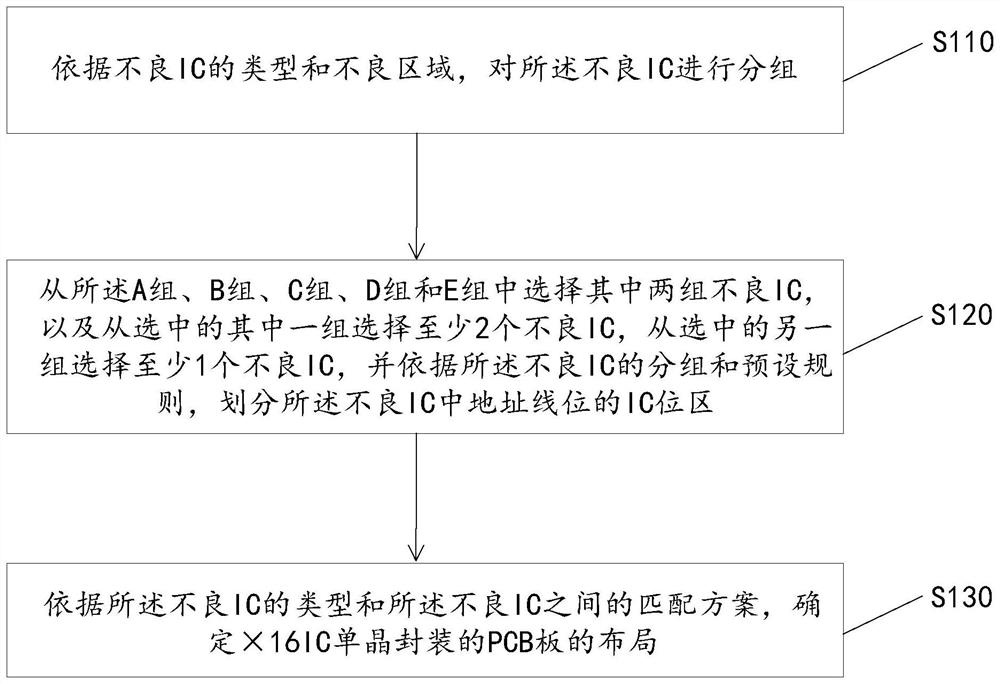
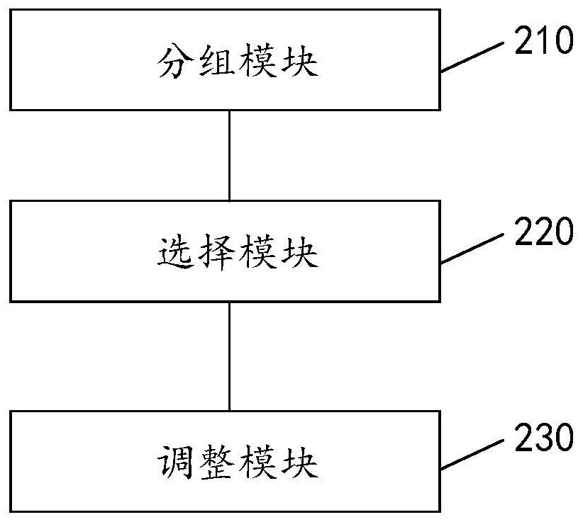
[0047] In order to make the purpose, features and advantages of the present application more obvious and understandable, the present application will be further described in detail below in conjunction with the accompanying drawings and specific implementation methods. Apparently, the described embodiments are some of the embodiments of the present application, but not all of them. Based on the embodiments in this application, all other embodiments obtained by persons of ordinary skill in the art without creative efforts fall within the protection scope of this application.

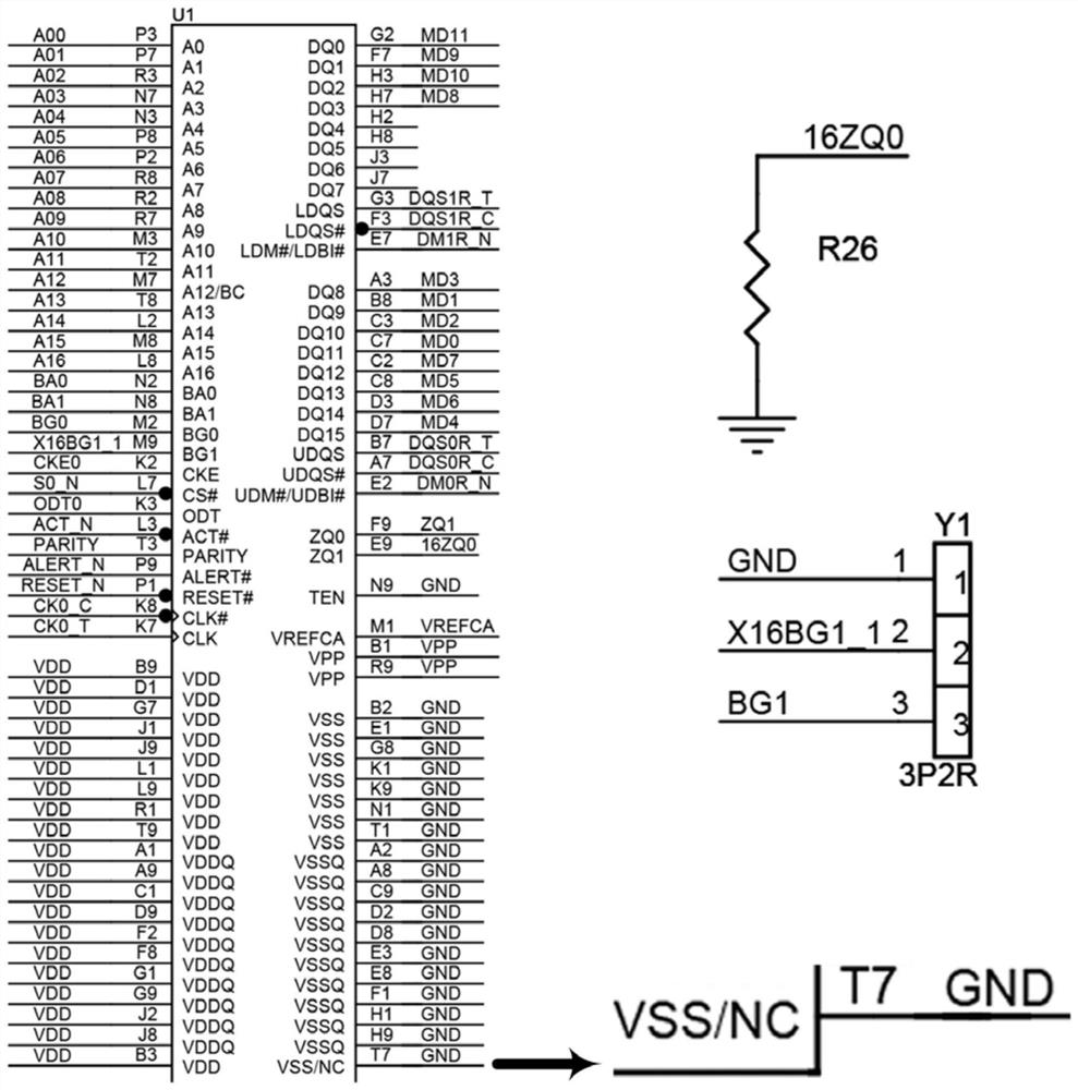
[0048]It should be noted that, in any embodiment of the present invention, the SDP encapsulation of the memory is that a Package contains a Die (referring to a memory particle, that is, a memory IC), that is, an SDP (Signle-Die Package), and the capacity is still It is the capacity size of a memory granule. DDP is a Package that contains 2 Dies, that is, the packaging method of DDP (Dual-Die Package). At...


PUM


Abstract

The invention provides a method and device for repairing a single-crystal memory, and the method comprises the steps: carrying out the grouping of bad ICs according to the types and bad regions of the bad ICs; selecting two groups of bad ICs from the group A, the group B, the group C, the group D and the group E, selecting at least two bad ICs from one selected group, selecting at least one bad IC from the other selected group, and dividing IC bit areas of address line bits in the bad ICs according to grouping of the bad ICs and a preset rule; and according to the IC bit area and the type of the bad IC, adjusting the layout of the PCB packaged by the * 16 IC single crystal. By means of the method, the SDP type packaged memory of the defective product can be repaired, the defective product existing in the factory memory IC is utilized, the defective product is changed into a qualified product through repairing, the defective product is effectively utilized, resources are saved, and meanwhile environment protection is facilitated to a certain degree.

Description

technical field [0001] The present application relates to the technical field of memory chips, in particular to a method, device and equipment for repairing single crystal memory. Background technique [0002] Memory, also known as random access memory (English: Random Access Memory, abbreviation: RAM), also called main memory, is an internal memory that directly exchanges data with the CPU. It can be read and written at any time (except when refreshing), and the speed is very fast, and it is usually used as a temporary data storage medium for operating systems or other running programs. When RAM is working, information can be written (stored) or read (taken out) from any specified address at any time. The biggest difference between it and ROM is the volatility of data, that is, the stored data will be lost once the power is turned off. RAM is used in computers and digital systems to temporarily store programs, data, and intermediate results. [0003] However, memory manu...

Claims


Application Information

Patent Timeline
IPC IPC(8): G11C29/00G11C29/18
CPCG11C29/88G11C29/18
Inventor 张丽丽陈任佳李苑锋林劲涛
Owner SHENZHEN JIAHE JINWEI ELECTRONICS TECH
Features
  • Generate Ideas
  • Intellectual Property
  • Life Sciences
  • Materials
  • Tech Scout
  • Unparalleled Data Quality
  • Higher Quality Content
  • 60% Fewer Hallucinations
Learn More