Supercharge Your Innovation With Domain-Expert AI Agents!

Silicon wafer turning device for silicon wafer electrode printing

A technology of electrode and flipping, which is applied in the manufacture of circuits, electrical components, semiconductors/solid-state devices, etc. It can solve the problems of reducing the efficiency of silicon wafer printing flipping, time-consuming and laborious, and the production efficiency of silicon wafer printing products, etc., to achieve convenient and automatic fixing , improve flipping efficiency, and improve the effect of diversity

Pending Publication Date: 2022-03-01
湖南泰安硅业有限公司
View PDF0 Cites 0 Cited by
  • Summary
  • Abstract
  • Description
  • Claims
  • Application Information

AI Technical Summary

Problems solved by technology

[0004] In view of the above situation, in order to overcome the defects of the prior art, the present invention provides a flipping device for electrode printing on silicon wafers, which effectively solves the need for staff to flip the two sides of silicon wafers intermittently in the

Method used


Image

  • Silicon wafer turning device for silicon wafer electrode printing
  • Silicon wafer turning device for silicon wafer electrode printing
  • Silicon wafer turning device for silicon wafer electrode printing

Examples


Embodiment 1

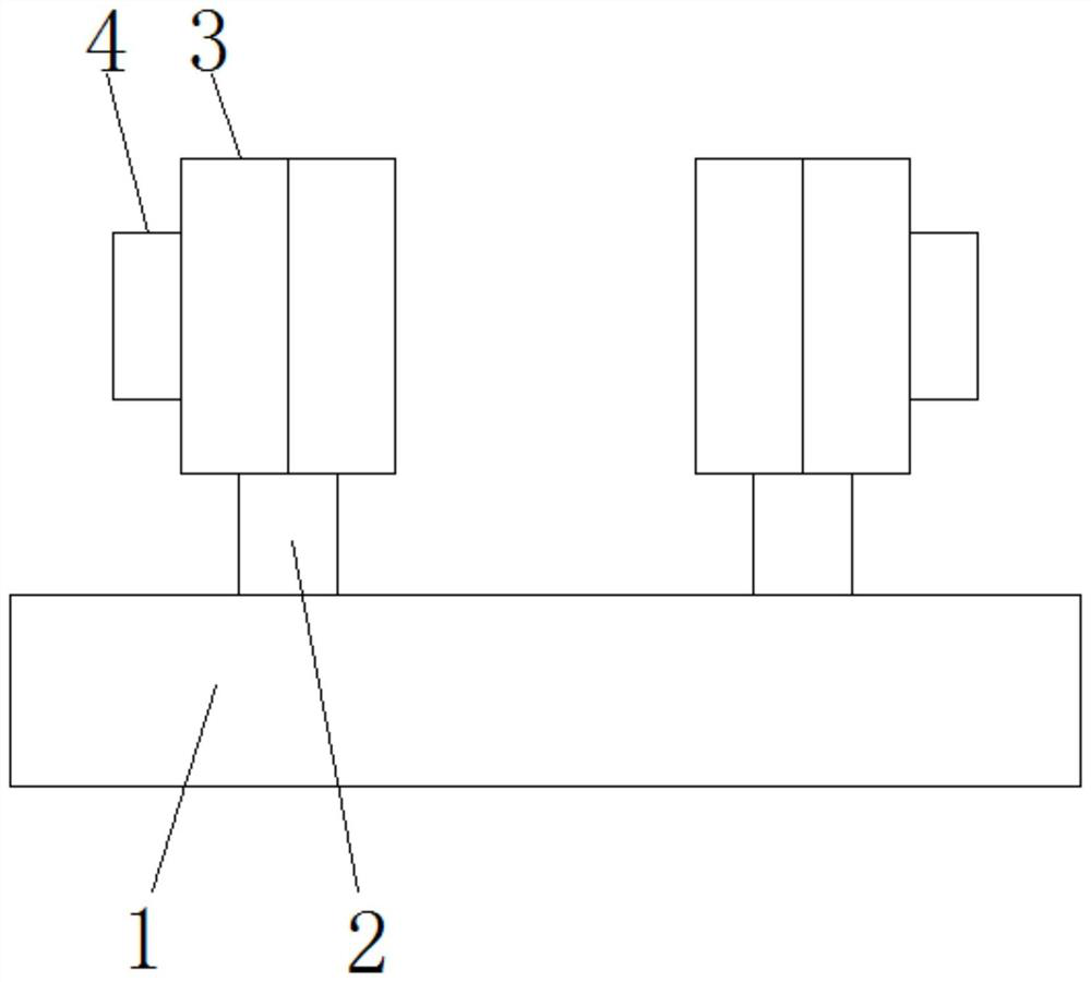
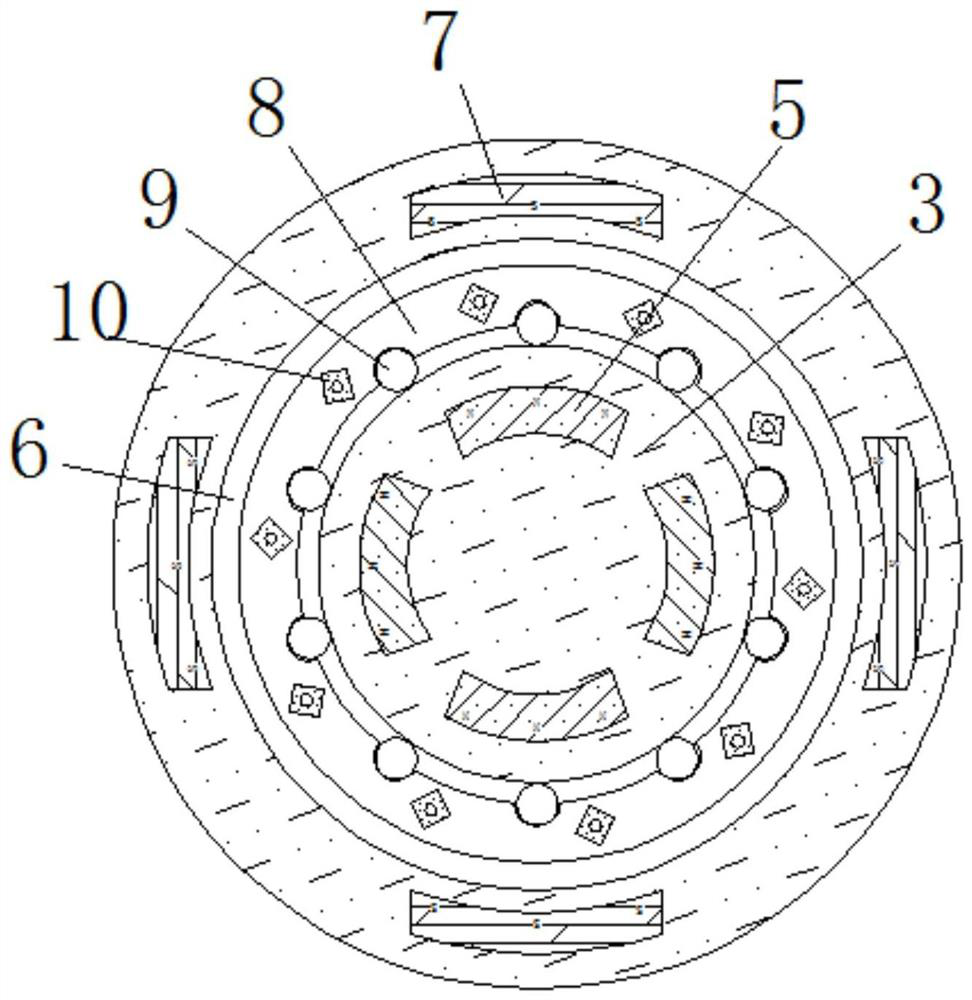
[0026] Embodiment one, by Figure 1-6 Given, the present invention includes a flipping device for silicon wafer electrode printing, including a working platform 1, the top of the working platform 1 is fixedly connected with a support column 2, and the outer side of the support column 2 is fixedly connected with a fixed plate 3, and the fixed plate The inwall of 3 is movably connected with rotating disk 4, the inwall of fixed disk 3 is fixedly connected with magnet one 5, the inwall of fixed disk 3 is provided with ring groove 6, the inwall of fixed disk 3 and the outside near ring groove 6 is fixedly connected with magnet two 7. The magnetism of the opposite surface of magnet one 5 and magnet two 7 is opposite, the quantity of magnet one 5 is the same as the quantity of magnet two 7, and magnet one 5 and magnet two 7 have played the effect of generating magnetic field;

[0027] The inner side of the ring groove 6 is movably connected with a swivel 8, and the swivel 8 plays the...

Embodiment 2

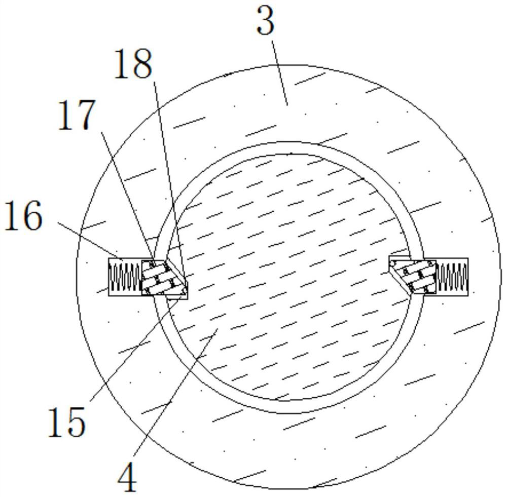
[0030] Embodiment 2. On the basis of Embodiment 1, the present invention includes a flipping device for electrode printing on silicon wafers, including a working platform 1. The top of the working platform 1 is fixedly connected with a supporting column 2, and the outer side of the supporting column 2 is Fixedly connected with a fixed disk 3, the inner wall of the fixed disk 3 is movably connected with a rotating disk 4, the inner wall of the fixed disk 3 is fixedly connected with a magnet-5, the inner wall of the fixed disk 3 is provided with a ring groove 6, and the inner wall of the fixed disk 3 is close to the ring. The outside of groove 6 is fixedly connected with magnet two 7, and the magnetism of the opposite surface of magnet one 5 and magnet two 7 is opposite, and the quantity of magnet one 5 is identical with the quantity of magnet two 7, and magnet one 5 and magnet two 7 have played the effect of generating magnetic field effect;

[0031] The inner side of the ring ...


PUM


Abstract

The invention relates to the technical field of silicon wafer manufacturing, and discloses a wafer turning device for silicon wafer electrode printing, which comprises a working platform, a supporting column is fixedly connected to the top of the working platform, a fixed disc is fixedly connected to the outer side of the supporting column, and a rotating disc is movably connected to the inner wall of the fixed disc. A first magnet is fixedly connected to the inner wall of the fixing disc, an annular groove is formed in the inner wall of the fixing disc, a second magnet is fixedly connected to the position, close to the outer side of the annular groove, of the inner wall of the fixing disc, and a rotating ring is movably connected to the inner side of the annular groove. According to the wafer turning device for silicon wafer electrode printing, in the working process, the first magnet, the second magnet and the rotating ring arranged in a matched mode are arranged, the rotating ring is driven to rotate through Ampere force borne by a conductive rod, the two faces of a silicon wafer are mechanically turned over, the situation that a worker needs to fix the silicon wafer again is avoided, time and labor are saved, and the working efficiency is improved. The overturning efficiency of silicon wafer printing is improved, and the production efficiency of silicon wafer printing products is improved.

Description

technical field [0001] The invention belongs to the technical field of silicon wafer manufacturing, in particular to a wafer turning device used for silicon wafer electrode printing. Background technique [0002] Silicon wafers made of silicon materials are commonly used in computer chips in the computer field. No matter how complicated the mathematical problems, physical problems and engineering problems are, and no matter how much the calculation workload is, the staff only need to tell it the problem through the computer keyboard. And issue ideas and instructions to solve the problem, the computer can tell you the answer in a very short time, so that the computer may only need a few minutes to solve the problems that take years or decades to calculate manually. During the manufacturing process of existing silicon wafers, electrodes need to be printed on the silicon wafers. [0003] However, in the process of printing electrodes on the silicon wafers currently on the mark...

Claims


Application Information

Patent Timeline
IPC IPC(8): H01L21/687
CPCH01L21/68792
Inventor 张立亮熊吉伟潘瑞林田昌勇黄梓
Owner 湖南泰安硅业有限公司
Features
  • R&D
  • Intellectual Property
  • Life Sciences
  • Materials
  • Tech Scout
  • Unparalleled Data Quality
  • Higher Quality Content
  • 60% Fewer Hallucinations
Learn More