Processing method for transparent area of glass substrate coated with AG layer

A glass substrate and transparent area technology is applied in the processing field of the transparent area of ​​the glass substrate, which can solve the problems of easy occurrence of defective products, affecting the appearance of products, and difficulty in controlling the grinding process. Effect

Pending Publication Date: 2022-03-25
ACETECH ELECTRONICS IND XIAMEN
View PDF0 Cites 0 Cited by
  • Summary
  • Abstract
  • Description
  • Claims
  • Application Information

AI Technical Summary

Problems solved by technology

The screen part of the resistive touch screen is a multi-layer composite film that matches the surface of the display, with a layer of glass or plexiglass as the base layer, generally called a glass substrate, and the surface of the glass substrate is coated with an AG layer. Anti-glare function, but there are generally some transparent areas around the touch screen. These transparent areas are used to display the status of some touch screens, such as displaying power status, temperature, etc. according to requirements. The glass substrate corresponding to this part of the transparent area cannot be covered by the AG layer. Coating and covering, in order to achieve this effect, the existing manufacturing process mainly has two processing methods, one: place a covering layer on the transparent area, such as sticking glue on the transparent area, and then apply the AG layer, coating After the end, tear off the glue, but the process of tearing off the glue tends to leave burrs on the periphery of the remaining AG layer, which affects the appearance of the product; secondly, after the AG layer is coated, use a jig to grind the transparent area, but the grinding The strength of the process is not easy to control, and defective products are prone to appear

Method used


Image

  • Processing method for transparent area of glass substrate coated with AG layer

Examples


Embodiment Construction

[0015] The present invention will be described in detail below in conjunction with the accompanying drawings and specific embodiments.

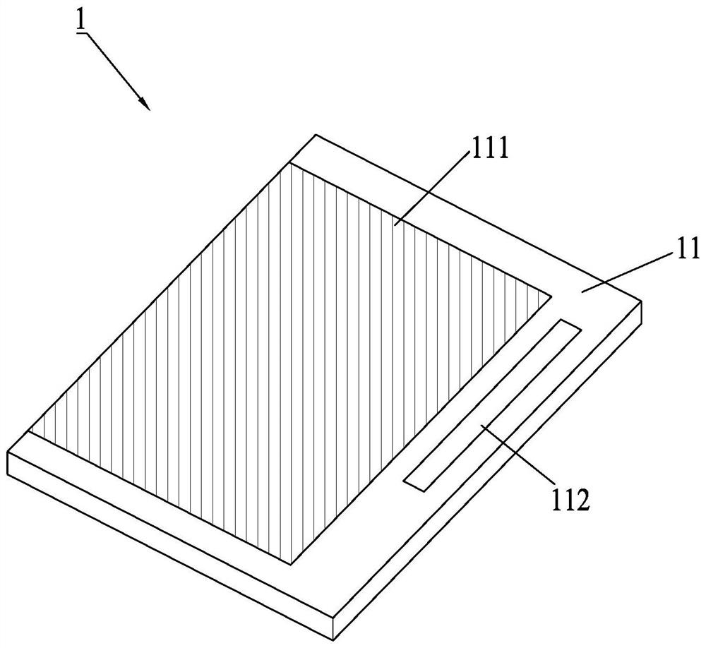
[0016] Such as figure 1 As shown, the front surface 11 of the glass substrate 1 is provided with a touch screen 111 and a transparent area 112;

[0017] A processing method for a transparent region of a glass substrate coated with an AG layer, characterized in that it comprises the following processes:

[0018] Step 1: Printing a circuit on the front surface 11 of the glass substrate 1 by screen printing, and coating ink on the transparent area 112 of the glass substrate 1, and the ink is a curing agent with a weight content of 1-3%;

[0019] Step 2: Baking the ink to make it dry; the temperature of the baking ink is 130-150°C, and the baking time is 5-15 minutes;

[0020] Step 3: Coating an AG layer on the entire front surface 11 of the glass substrate 1:

[0021] Step 4: Clean the front surface 11 of the glass substrate 1 again by ultras...


PUM


Abstract

A processing method for a transparent area of a glass substrate coated with an AG layer comprises the following steps that firstly, the front surface of the glass substrate is printed with printing ink through a screen printing plate, the transparent area of the glass substrate is coated with the printing ink, and the printing ink is printing ink without a curing agent or printing ink with a low curing agent; 2, baking the printing ink to dry the printing ink; step 3, coating the whole front surface of the glass substrate with an AG layer; and step 4, cleaning the front surface of the glass substrate, and cleaning the ink and the AG layer above the ink to expose a transparent area. According to the invention, the characteristic that the ink without or with little curing agent is easy to clean is utilized, the process is simple, cleaning is very clean, and burrs are not left on the edge of the remaining coated AG layer after cleaning, so that the edge is neat and clear; in addition, the printing ink without or with less curing agent is convenient to clean, and the transparent area is not abraded in the cleaning process, so that the yield is greatly improved.

Description

technical field [0001] The invention relates to the display screen manufacturing industry, in particular to a processing method for the transparent area of ​​a glass substrate coated with an AG layer. Background technique [0002] As a kind of human-computer interaction interface, touch screen has entered various fields, especially widely used in portable electronic equipment and public inquiry equipment. A resistive touch screen is a sensor that converts the physical position of a touch point (X, Y) in a rectangular area into a voltage representing the X-axis coordinates and the Y-axis coordinates. Many Liquid Crystal Display (LCD) modules use Resistive touch screen. The screen part of the resistive touch screen is a multi-layer composite film that matches the surface of the display, with a layer of glass or plexiglass as the base layer, generally called a glass substrate, and the surface of the glass substrate is coated with an AG layer. Anti-glare function, but there ar...

Claims


Application Information

Patent Timeline
IPC IPC(8): G06F3/045
CPCG06F3/045G06F2203/04103
Inventor 朱绍兴
Owner ACETECH ELECTRONICS IND XIAMEN
Why Eureka
Try Eureka