Memory cell group and manufacturing method thereof

A technology of memory cells and manufacturing methods, applied in electrical components, semiconductor devices, circuits, etc., can solve the problems of long metal wires and low integration of resistive memory, reduce the wire length by half, meet the needs of miniaturization, improve The effect of storage capacity

Pending Publication Date: 2022-03-25
XIAMEN IND TECH RES INST CO LTD
View PDF5 Cites 0 Cited by
  • Summary
  • Abstract
  • Description
  • Claims
  • Application Information

AI Technical Summary

Problems solved by technology

[0003] The resistive memory with the above-mentioned structure has a low integration level. If the component integration level is increased in a planar manner, the chip area must be enlarged. However, the current demand for semiconductor devices tends to be miniaturized, and the space for expanding the chip area is very large.
[0004] In addition, 1T1R memory cells will result in longer metal wires, resulting in IR drop (IR drop) phenomenon

Method used


Image

  • Memory cell group and manufacturing method thereof
  • Memory cell group and manufacturing method thereof
  • Memory cell group and manufacturing method thereof

Examples


Embodiment Construction

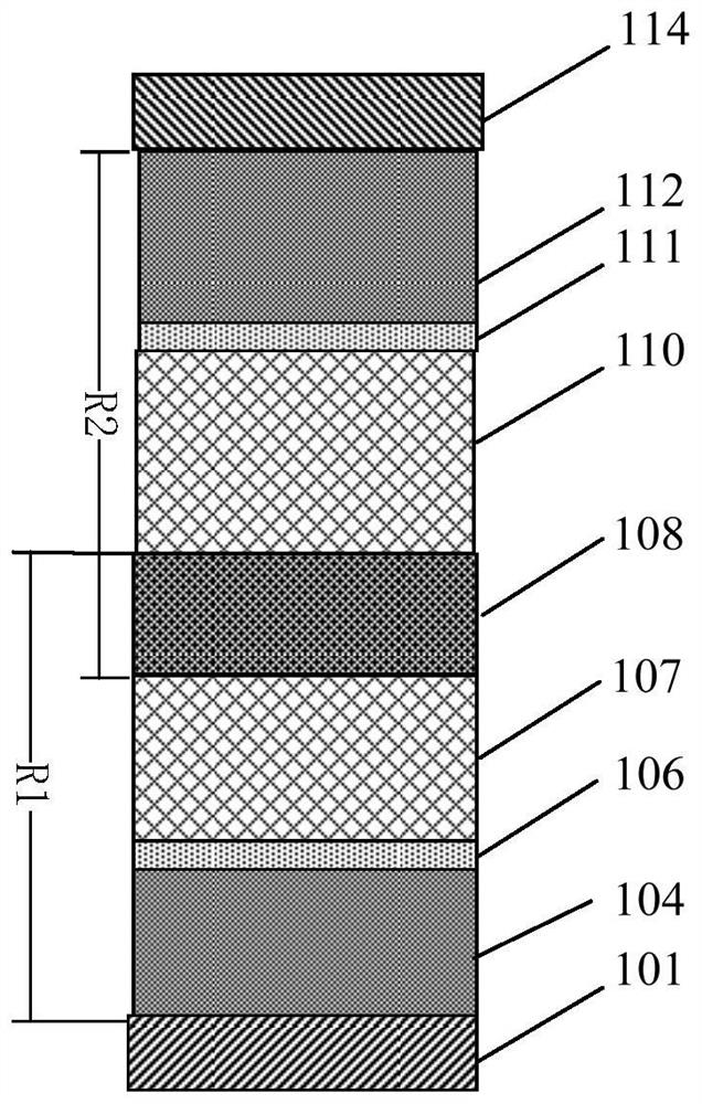
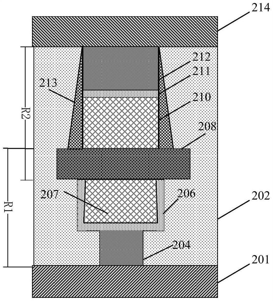
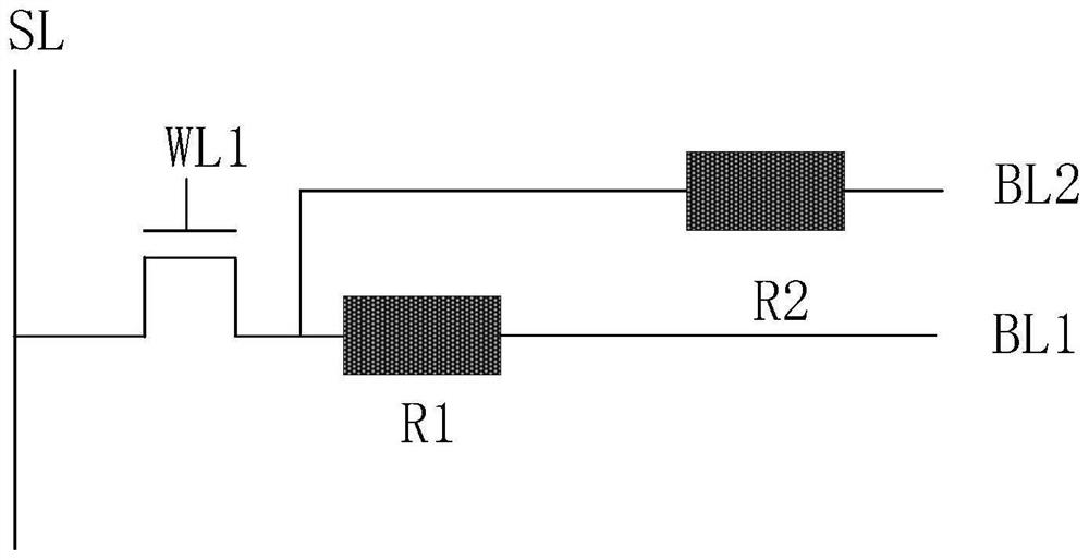
[0048] In order to make the purpose, features, and advantages of the application more obvious and understandable, the technical solutions in the embodiments of the application will be clearly and completely described below in conjunction with the accompanying drawings in the embodiments of the application. Obviously, the described The embodiments are only some of the embodiments of the present application, but not all of them. Based on the embodiments in this application, all other embodiments obtained by those skilled in the art without making creative efforts belong to the scope of protection of this application.

[0049] In the description of this specification, descriptions referring to the terms "one embodiment", "some embodiments", "example", "specific examples", or "some examples" mean that specific features described in connection with the embodiment or example , structure, material or characteristic is included in at least one embodiment or example of the present applic...


PUM


Abstract

The invention discloses a memory cell group and a manufacturing method thereof, and the memory cell group shares an electrode between an upper resistive memory cell and a lower resistive memory cell, and shares a line through the electrode. And then, another non-shared electrode is connected to different lines, so that two resistive random access memory units which are overlapped up and down and can be independently controlled are realized. On one hand, the storage unit group can form a 1T2R storage unit array, and the number of the storage units can be greatly increased on the premise that the number of transistors is not increased, so that the storage capacity of a system is improved; on the other hand, by sharing one electrode, the space of one electrode can be saved, and the requirement for element miniaturization is better met. Besides, in the array with the same element integration level, the length of the wire can be halved by the double-layer stacked structure, so that the IR drop is greatly reduced.

Description

technical field [0001] The present application relates to the field of semiconductor devices, in particular to a memory unit group and a manufacturing method thereof. Background technique [0002] The basic structure of a resistive random access memory (RRAM) includes a top electrode, a resistive layer and a bottom electrode, and usually uses 1T1R memory cells stacked layer by layer from bottom to top. [0003] The resistive memory with the above-mentioned structure has a low integration level. If the component integration level is increased in a planar manner, the chip area will inevitably need to be enlarged. However, the current demand for semiconductor devices tends to be miniaturized, and the space for expanding the chip area is very large. [0004] In addition, the 1T1R memory cell will lead to a longer metal wire, thus causing an IR drop (IR drop) phenomenon. Contents of the invention [0005] In view of the above technical problems, the applicant creatively provid...

Claims


Application Information

Patent Timeline
IPC IPC(8): H01L27/24
CPCH10B63/845H10B63/84
Inventor 邱泰玮单利军沈鼎瀛
Owner XIAMEN IND TECH RES INST CO LTD
Why Eureka
Try Eureka