
Packaging circuit structure and manufacturing method thereof

A technology for encapsulating circuits and manufacturing methods, which is applied in the direction of circuits, radiating element structural forms, antenna grounding switch structural connections, etc., and can solve problems such as lightness, thinness, and shortness of electronic products, occupying space of electronic products, and affecting the volume of electronic products, etc. , achieve the effect of improving heat dissipation and avoiding electromagnetic interference

Pending Publication Date: 2022-04-01
AVARY HLDG (SHENZHEN) CO LTD +1
View PDF0 Cites 0 Cited by
  • Summary
  • Abstract
  • Description
  • Claims
  • Application Information

AI Technical Summary

Problems solved by technology

As the main component of electronic products, the circuit structure occupies a large space of electronic products. Therefore, the volume of the circuit structure affects the volume of electronic products to a large extent. short and small trend

Method used


Image

  • Packaging circuit structure and manufacturing method thereof
  • Packaging circuit structure and manufacturing method thereof
  • Packaging circuit structure and manufacturing method thereof

Examples


Embodiment Construction

[0067] The following will clearly and completely describe the technical solutions in the embodiments of the present invention with reference to the accompanying drawings in the embodiments of the present invention. Obviously, the described embodiments are only some, not all, embodiments of the present invention. Based on the embodiments of the present invention, all other embodiments obtained by persons of ordinary skill in the art without making creative efforts belong to the protection scope of the present invention.

[0068] Unless otherwise defined, all technical and scientific terms used herein have the same meaning as commonly understood by one of ordinary skill in the technical field of the invention. The terms used herein in the description of the present invention are for the purpose of describing specific embodiments only, and are not intended to limit the present invention.

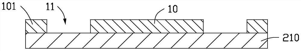
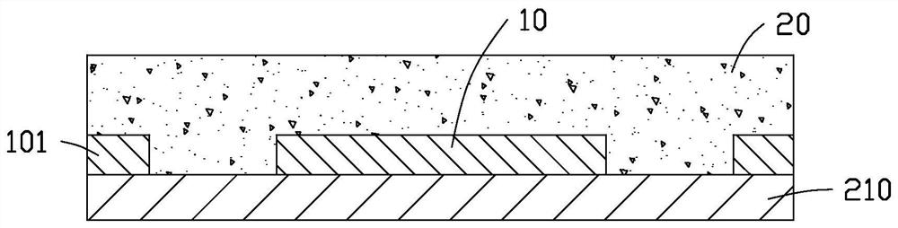
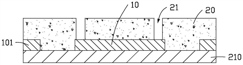
[0069] see Figure 1 to Figure 16 , the manufacturing method of the packaging circuit stru...


PUM


Abstract

A packaging circuit structure comprises a shielding layer, an electronic element, a plurality of conductive columns, a first insulating layer, a first circuit board, an antenna structure and a second circuit board. The shielding layer is provided with a groove. The electronic component is fixed in the groove. The plurality of conductive columns surround the groove and are arranged on the shielding layer. The first insulating layer wraps the shielding layer, the electronic element and the plurality of conductive columns. The first circuit board is stacked on one side of the first insulating layer. The first circuit board comprises a grounding wire, and the grounding wire is electrically connected with the plurality of conductive columns. The antenna structure is stacked on the side, away from the first insulating layer, of the first circuit board and is electrically connected with the electronic component through the first circuit board. The second circuit board is stacked on the side, away from the first circuit board, of the first insulating layer. The packaging circuit structure is beneficial to avoiding electromagnetic interference and improving the heat dissipation effect. The invention further provides a manufacturing method of the packaging circuit structure.

Description

technical field [0001] The invention relates to a packaging circuit structure and a manufacturing method thereof, in particular to a packaging circuit structure with an antenna structure and a manufacturing method thereof. Background technique [0002] In recent years, electronic products are widely used in daily work and life, and light, thin and small electronic products are becoming more and more popular. As the main component of electronic products, circuit structure occupies a large space of electronic products. Therefore, the volume of circuit structure affects the volume of electronic products to a large extent. Short and small trends. [0003] The existing antenna packaging technology (such as AoC, AiP) integrates antenna modules of different frequency bands and various RF chips / active components into the package structure, but how to avoid electromagnetic interference between RF ICs / active components has become an urgent problem to be solved important topic. In a...

Claims


Application Information

Patent Timeline
IPC IPC(8): H01L23/552H01L23/367H01L21/52H01L23/66H01Q1/22H01Q1/38H01Q1/50
CPCH01L23/3677H01L23/66H01L2224/32245H01L2924/3025H01L2924/15153H01L2223/6677H01L23/552H01L2224/04105H01L2224/12105H01L2224/73267H01L2224/92244H01L23/3121H01L24/19H01L24/83H01L21/4882H01L24/29
Inventor 魏永超李嘉禾
Owner AVARY HLDG (SHENZHEN) CO LTD
Features
  • Generate Ideas
  • Intellectual Property
  • Life Sciences
  • Materials
  • Tech Scout
  • Unparalleled Data Quality
  • Higher Quality Content
  • 60% Fewer Hallucinations
Learn More